PCB herstellen
Das Erstellen Ihrer eigenen Leiterplatte kann Platz in Ihrem Projekt sparen und gleichzeitig einen professionellen Eindruck machen. In diesem Kapitel schlagen wir einige Workshops und Tipps vor.
- Einführung in die Gestaltung von Leiterplatten mit KiCad
- KiCad Basics Tagebuch
- Assembly and Testing
- ZAM Badge 2024
- ZAM Badge - Cat with Knife
- Advent Löt-Aktion - Sternen
- ZAM Badge Löt-Bausäts
Einführung in die Gestaltung von Leiterplatten mit KiCad
Überblick
Teil 1. Ein Tag zum Erstellen eines Projekts mit KiCad - mit den Schaltplan- und PCB-Editoren sowie den Symbol- und Footprint-Editoren, um eine benutzerdefinierte Leiterplatte herzustellen.
Teil 2. Ein weitere Tag um die Platine zum Laufen zu bringen; Bestückung und Prüfung ist auch eingeplant.
Teilnehmer
Vorkenntnisse
Grundkenntnisse in Elektronik wären hilfreich aber nicht essentiell.
Mitbringen
Material Kosten
Am 2. Tag entstehen Materialkosten. Der genaue Beitrag ist abhängig von der PCB Größe. Ein Betrag zwischen 10€ bis 15€ ist zu erwarten.
Anmeldung
Ort
ZAM Hauptstrasse, Erlangen.
Programm
Tag 1 - Sa. 4. Juni 2022
Basic project creation up to layout.
|
Time |
Duration |
Topic |
|
10:00 |
30 |
COVID Testing. Introduction, house rules. |
|
10:30 |
45 |
Introduction to KiCad + Circuit Creation |
|
11:15 |
15 |
break |
|
11:30 |
45 |
Library Management - Symbols and Footprints |
|
12:15 |
60 |
Lunch |
|
13:15 |
45 |
Layout |
|
14:00 |
15 |
break |
|
14:15 |
45 |
Wrap up and packup |
|
15:00 |
finish |
Tag 2 - Sa. 25. Juni 2022
Assembly, testing and troubleshooting.
|
Time |
Duration |
Topic |
|
10:00 |
30 |
COVID Testing. Introduction, house rules. |
|
10:30 |
45 |
Assembly |
|
11:15 |
10 |
break |
|
11:25 |
45 |
Assembly |
|
12:10 |
60 |
Finish |
Designdateien
Die Designdateien sind auf dem GitHub Repository ZAM_KiCad_Basics erhältlich.
KiCad Basics Tagebuch
Teil 2. Samstag 25.06.22
The boards were not completed during the first session. A deadline to complete the boards was set for the 13.06.22 to ensure that the boards would be back in time for part 2. The order was posted 11.06.22 and the boards arrived back 20.06.22 so in plenty of time for part 2.
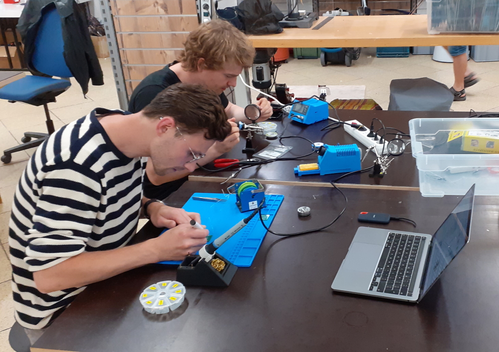
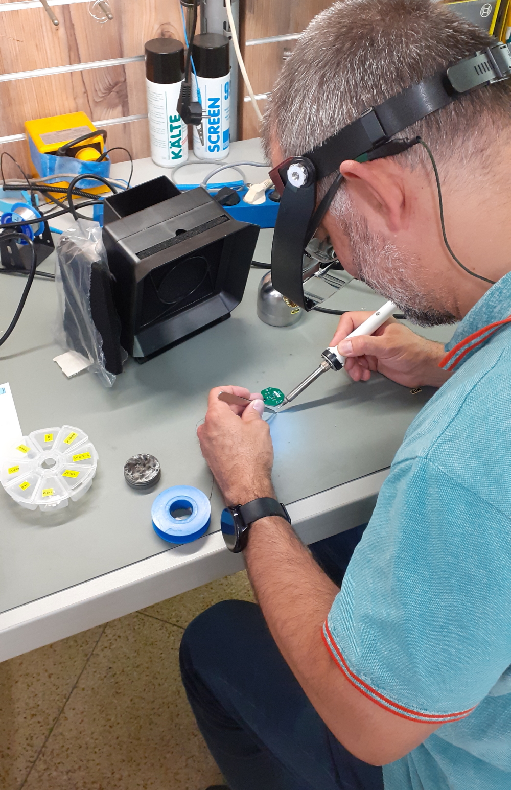
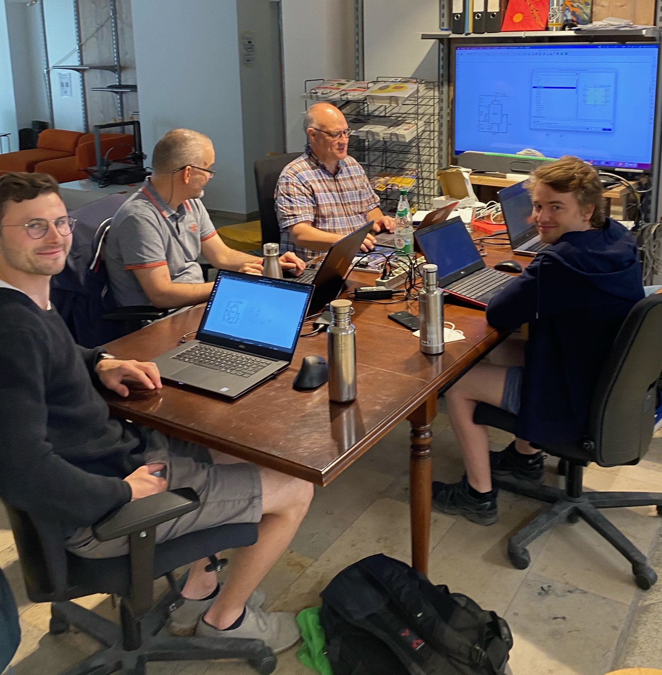
We started the day with a commentary on the layouts and some of the things to watch out for. Steve then demonstrated his approach to soldering Surface Mounted Devices (SMD). The smallest part is 2mm x 1.27mm. Once the approach was demonstrated, they were left to assemble their boards.
 |

|
|
Once assembly was completed, then it was time to test the work. All the boards worked without any issues.
 |
 |
 |
Things Learned and Improvements
The day went quite well. It was intended to be only a short session i.e. 2 hours and not as long as Part 1. Time-wise, it worked well and all were completed and packed up within 2½ hours. There is not much to consider to change in this case.
Teil 1. Samstag 04.06.22
Objective
The creation of projects in electronics requires the connection of various components to build a circuit. There are various means to achieve this - breadboard, verro-board. However there are many advantages to building an own Printed Circuit Board (PCB). The purpose of this workshop was to introduce the attendees to the KiCad electronic design tool so that they will gain the know-how and confidence to create their own PCBs.
There were two goals for the event.
- Introduce the attendees the work-steps required to create a PCB. This workflow is not unique to KiCad.
- Have a set of design files ready to send for fabrication.
Method
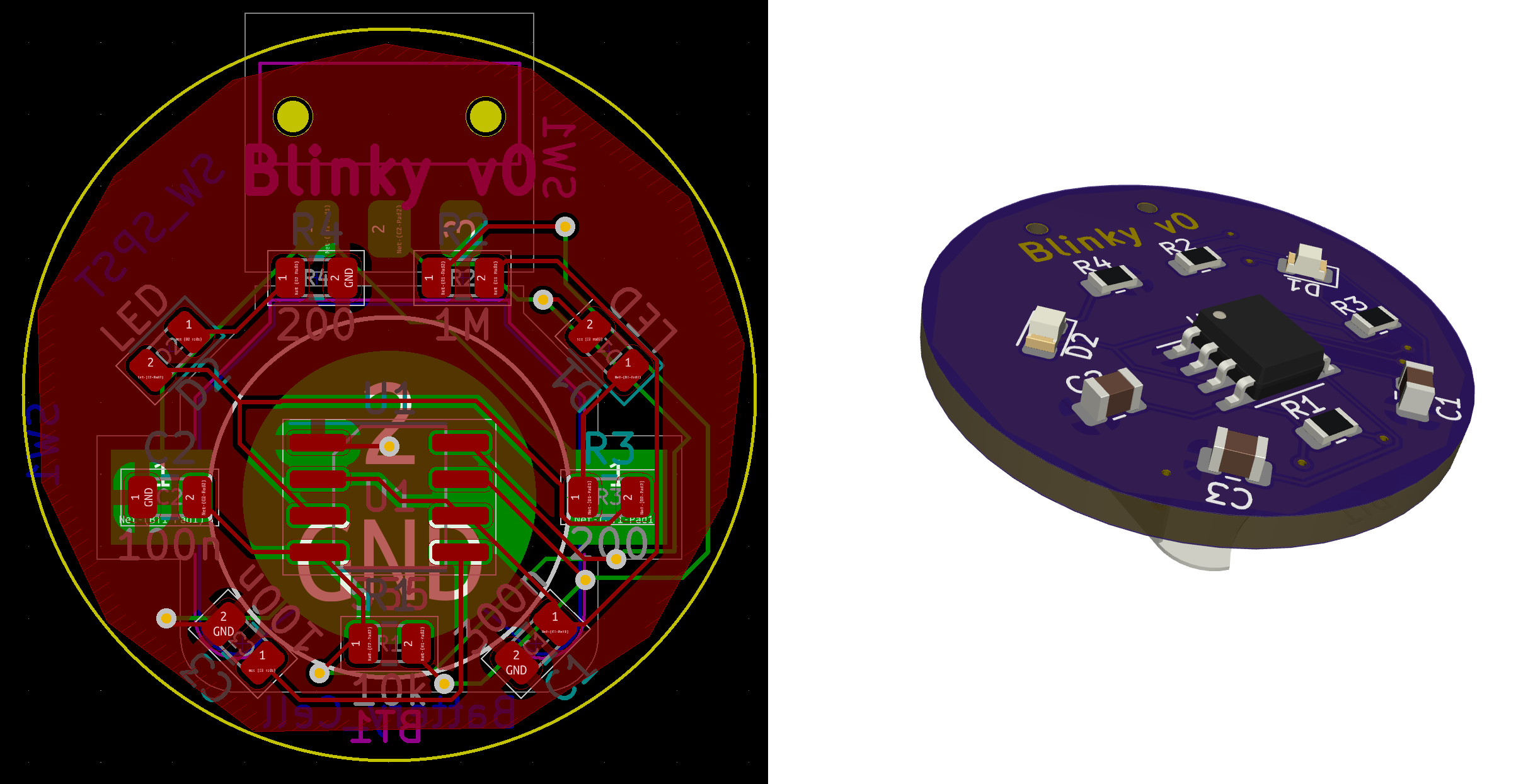
A relatively simple (but not too simple - Falstad model) project was presented. The classic first project, a blinking LED project. The project was presented as our final goal that we needed to implement as a PCB.

There was quite a bit of information to get through.
- Creating a project.
- Creating a schematic.
- Creating and modifying the symbols for a schematic.
- Assigning footprints to the symbols.
- Creating and modifying the footprints.
- Creating the layout.
Procedure
I opened the session with the question of why do we ant to create our own PCB? The answers that came back were consistent to what drew me into this area of electronic development.
- DIY home automation.
- Neatening up existing projects.
- Wanting to interface neatly with existing development boards.
- Create my own development board.
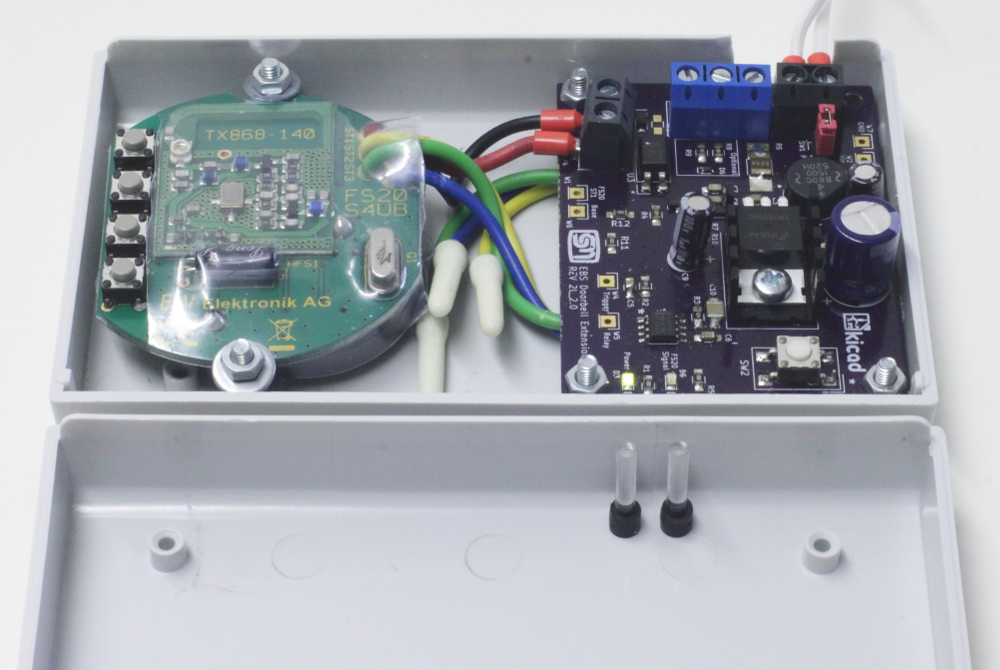
I showed my won example of neatening up a project. Where I presented a first attempt at creating my won door bell extension with what I knew at the time and using Verro board.
| Old | New |
 |
 |
We then started work. I introduced the software and the creation of the schematic diagram with an introduction to the symbol library and how you go about creating a new symbol or changing an existing one to suite the purpose of the diagram. It soon came apparent that a symbol does not need to exactly match the physical component that is going to be used in the circuit. The schematic is a design document to help the developer and other understand the operation of a circuit.
After lunch we moved onto the PCB Layout itself. Ideally the purpose of the class. I showed how to prepare the schematic for import into the PCB layout tool. The most important aspect being the footprints. A footprint is the physical form the component will take on the PCB. Each symbol must be associated to a footprint before the layout can be completed. The problem here is that for one symbol there could be any number of footprints to choose from. We need to consult the datasheet for the exact component we intend to purchase to ensure that out components will actually fit on our board and will be connect up correctly. This step should never be underestimated.
Another aspect of the layout I explained wat that we need to understand the design limitations and tolerances of the PCB fabrication house. Each house will have their own set of rules and we need to configure KiCad to help us adhere to those rules. This means we need to set up the minimum distances and widths allowed for the copper.
There is the question if this was a PCB creation workshop, how come we are preparing the design files to send off for fabrication? The answer is that the actual fabrication of the physical PCB is only one part of the process and actually not a significant part of the overall creative process of creating the design, assembling and troubleshooting. There is more than one technique for creating a PCB and ZAM does not yet have the facilities for either of these processes. Sending the boards off for fabrication is the simplest and most effective way to introduce the more important aspects of the creative process.
So at the end of the session, we now have some design files that can be sent off and on their return we will continue with the second part - the assembly and testing of the boards.
Things Learned and Improvements
This was the first KiCad workshop both for me and ZAM. In the planning it was important to me to make sure explain the design process workflow and highlight that at every stage of the process, we need to make design decisions. I consider this aspect is actually more important than the PCB software itself. However, I noticed there could have been a couple of tings done differently.
1. A Simpler project.
While the project itself seemed to be simple, and easy to explain, especially with Falstad Circuit, I tend to think now for a basic KiCad introduction, the concepts of symbol and footprint library management including symbol and footprint creation could be left off for a separate workshop.
2. Break the workshop up
While it was nice to have the full day to concentrate on the project, it was a long day and in the end the design files were not ready and had to be handed in a couple of days later. In thinking about point 1. above, with a simpler project, the workshop could be broken up into shorter, 2 hour, sessions that could be scheduled during an evening rather that taking up a whole day on the weekend. These session could then focus on specific aspects like the following list. The last three items are somewhat related but have differences that make them hard or too large to include in one session.
- Schematic Creation
- PCB Layout
- Library Management
- Managing a PCB project with GIT
- Adding graphics to a PCB
- Custom and Fun board shapes
- Artistic PCB i.e. Creating Blinking Badges
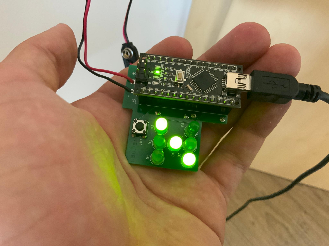
Assembly and Testing
Assembly and Testing
Overview
The assembly and testing of self-designed PCBs requires some extra equipment. Much of this has already been thought out on the Rapid Prototyping Elektronik page and in particular on the associated spreadsheet/list. I would like repeat some of the recommended items here. Another good reference for this is the Soldering Workshop presented by Binary Kitchen, Regensburg.
The kit for each attendee
- Lötstation
- Löt
- Schutzbrille
- Lötrauchabsaugung
- Metallschwamm
- Seitenschneider
- Pinzetten
- Drittehand
- Entlötpumpe und Entlötlitze
- ESD matte
- Lampe.
Advanced Gear
- Heißluftlötstation
- Reflow-ofen
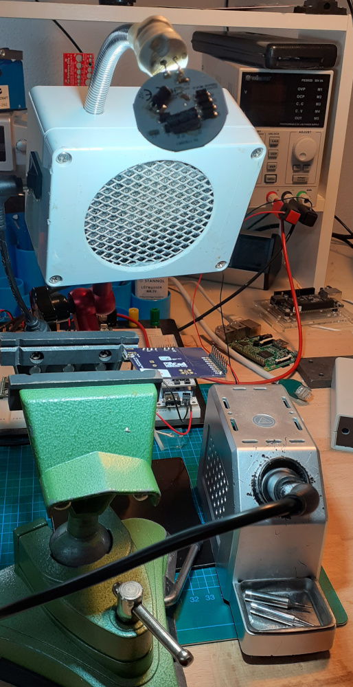
Some of this equipment is already in ZAM. However, there is not enough to run any type of soldering workshop and the safety equipment is as yet not available - solder fumes extractor and safety glasses.
We could build our own Solder fume extractor. Binary kitchen have theirs as a kit. There are plenty of other examples on the Thingiverse. In my case, I created one from a PC cooling fan, an off-the-shelf case, a 12 V LED lamp and a flexible hose from a fire-lighter. I imagine we could come up with something in the middle.
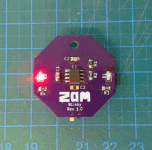
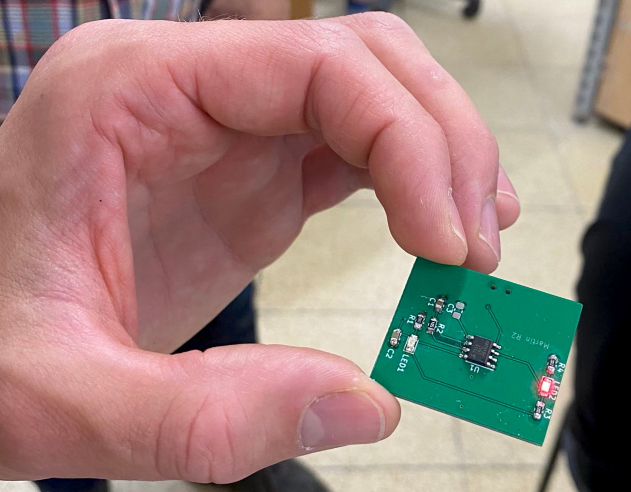
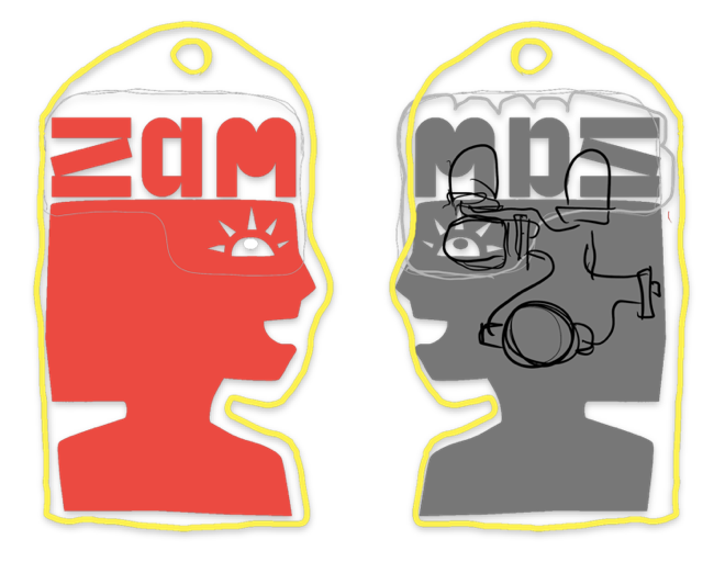
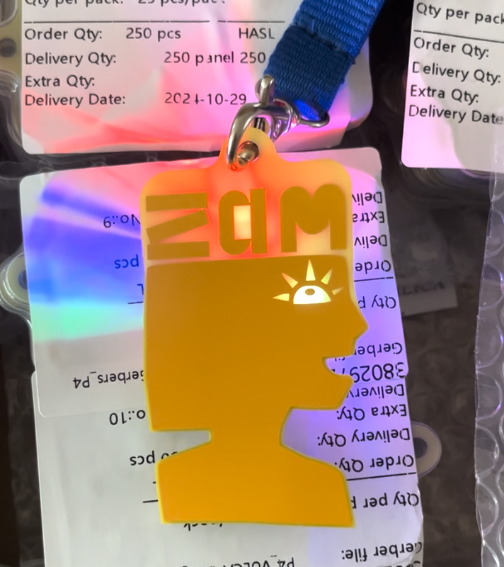
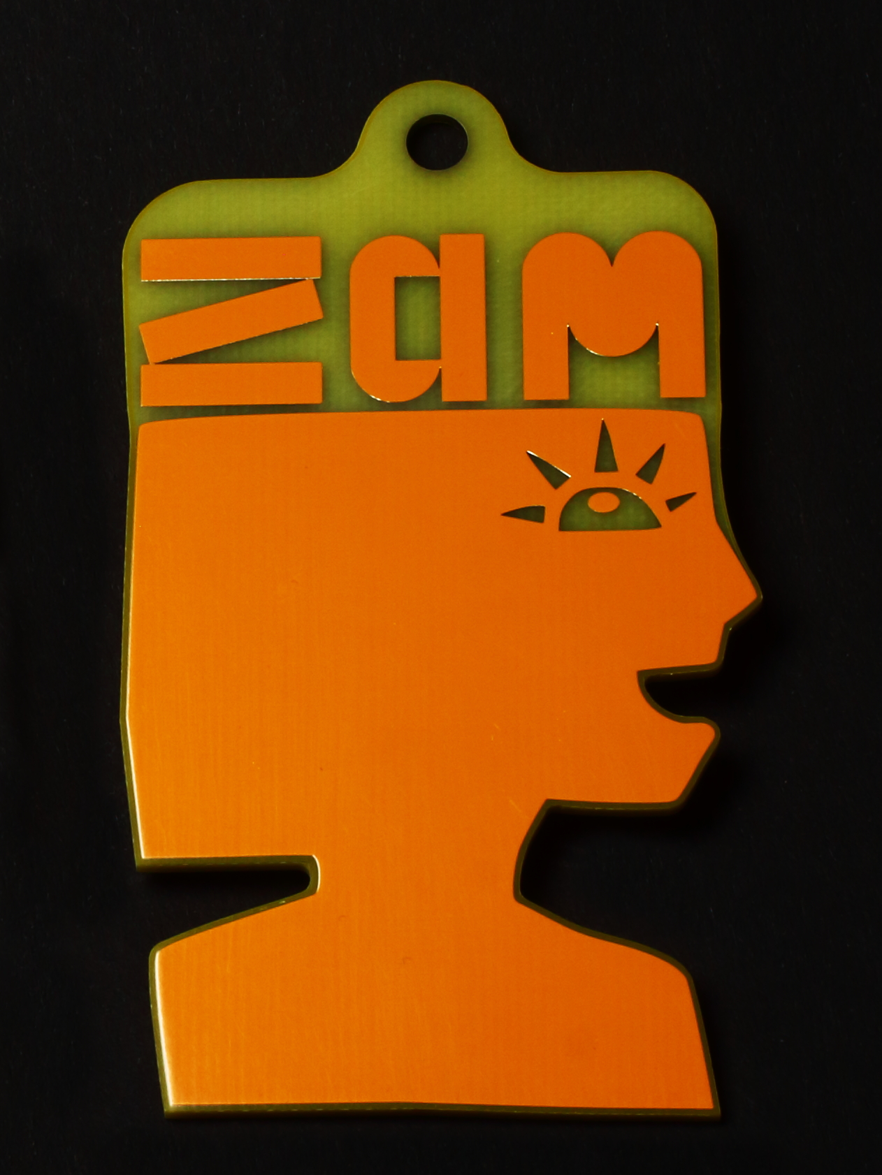
ZAM Badge 2024
Überblick
Bei der Planung des VULCA-Treffens kam die Idee eines Badge als Konferenzpräsent und Lötübung auf. Die Idee besteht darin, die folgende Grafik zu nehmen und diese in eine Leiterplatte mit blinkenden LEDs hinter dem Auge und den Buchstaben umzuwandeln.

Projekt-Metadaten
ZAM-Badge-24 GitHub Repository
Jochen Hunger jochen.hunger@betreiberverein.de
Steve Mayze smayze@yahoo.com
Logbuch / Schritte
Tag 1 Zusammenarbeit
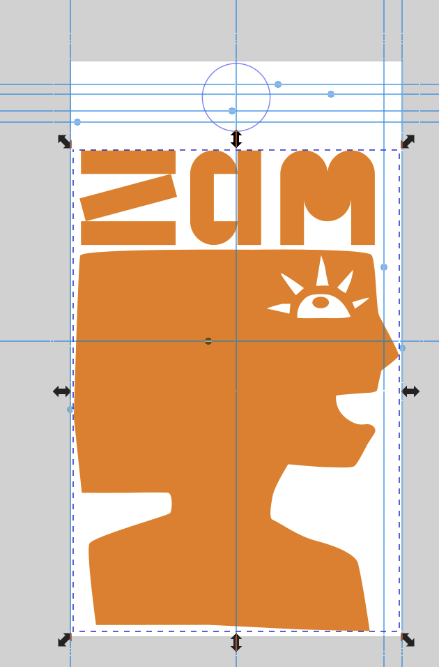
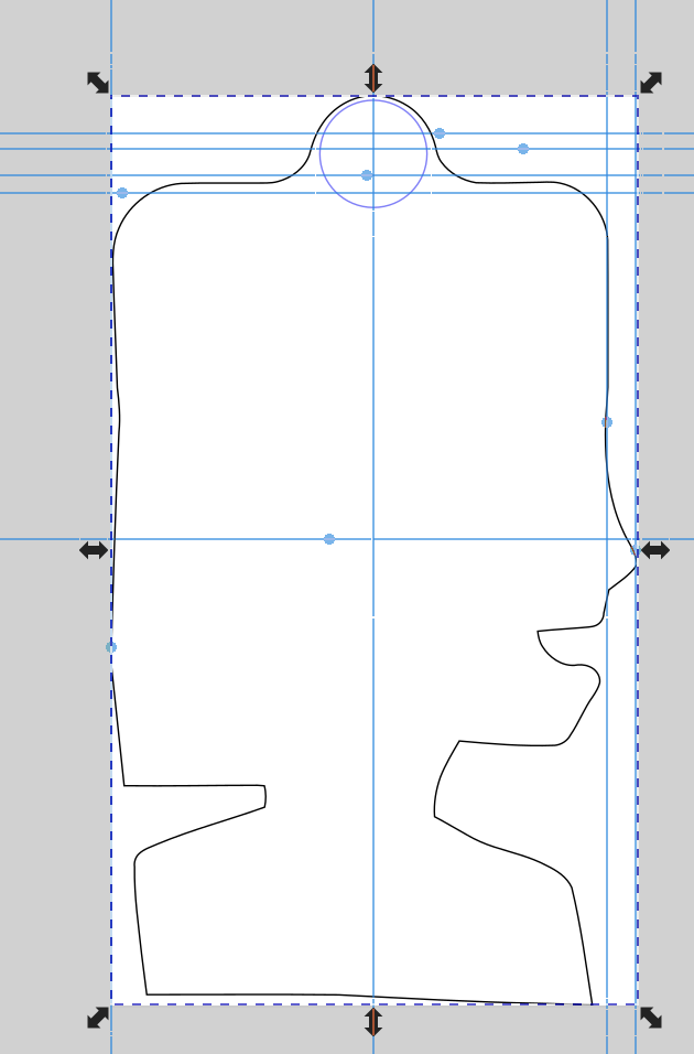
Ich habe schon früher Grafiken in PCBs umgewandelt. Ich wollte dieses Projekt unbedingt in Angriff nehmen, da ich einige Wochen zuvor an der KiCon Europe 2024 teilgenommen hatte und den Vortrag „Zusammenarbeit mit Künstlern, um schöne Platinen zu entwerfen“ sehr genossen hatte. Als Erstes musste ich mir das Konzept ausdenken. Auf Grundlage der Originalgrafik skizzierte ich eine mögliche Anordnung der PCB-Schichten.

Basierend auf dieser Skizze hat Jochen dann seine Vorstellungen dargelegt. Daraus ließe sich relativ einfach eine Leiterplatte entwickeln. Die Idee ist, Kopf und Buchstaben alle in der gleichen Farbe zu haben (die Lötmaske) und dann den Bereich hinter den Augen und um die Buchstaben herum frei zu lassen, damit die blinkenden LEDs hindurchscheinen.
 Ich habe dies noch etwas weiter ausgeschmückt und mir Gedanken darüber gemacht, wo die Komponenten platziert werden könnten.
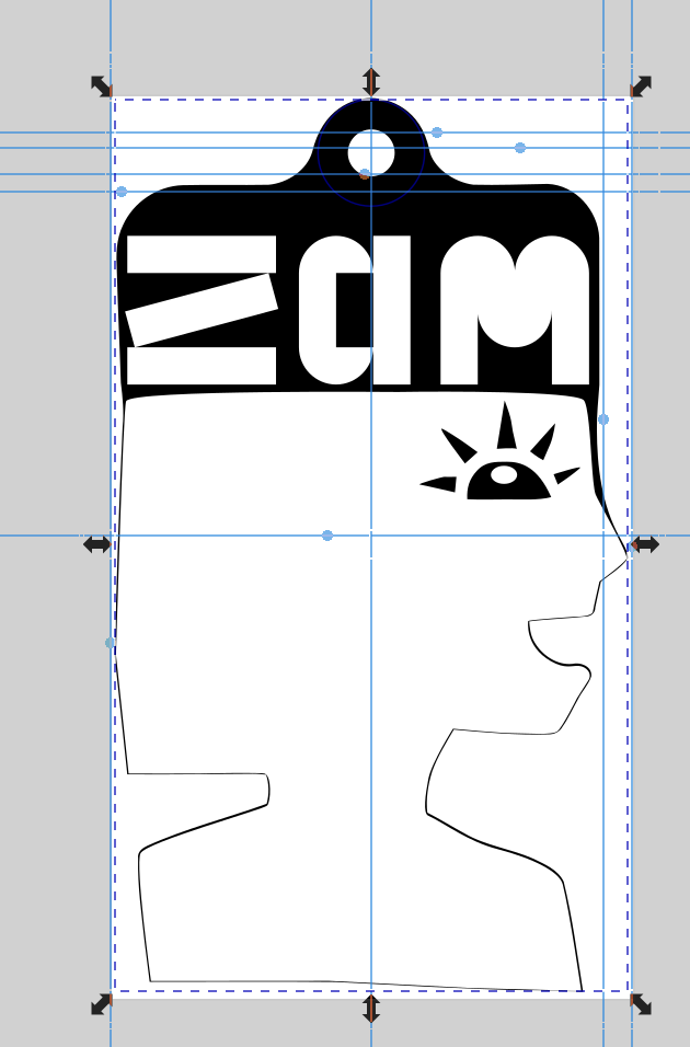
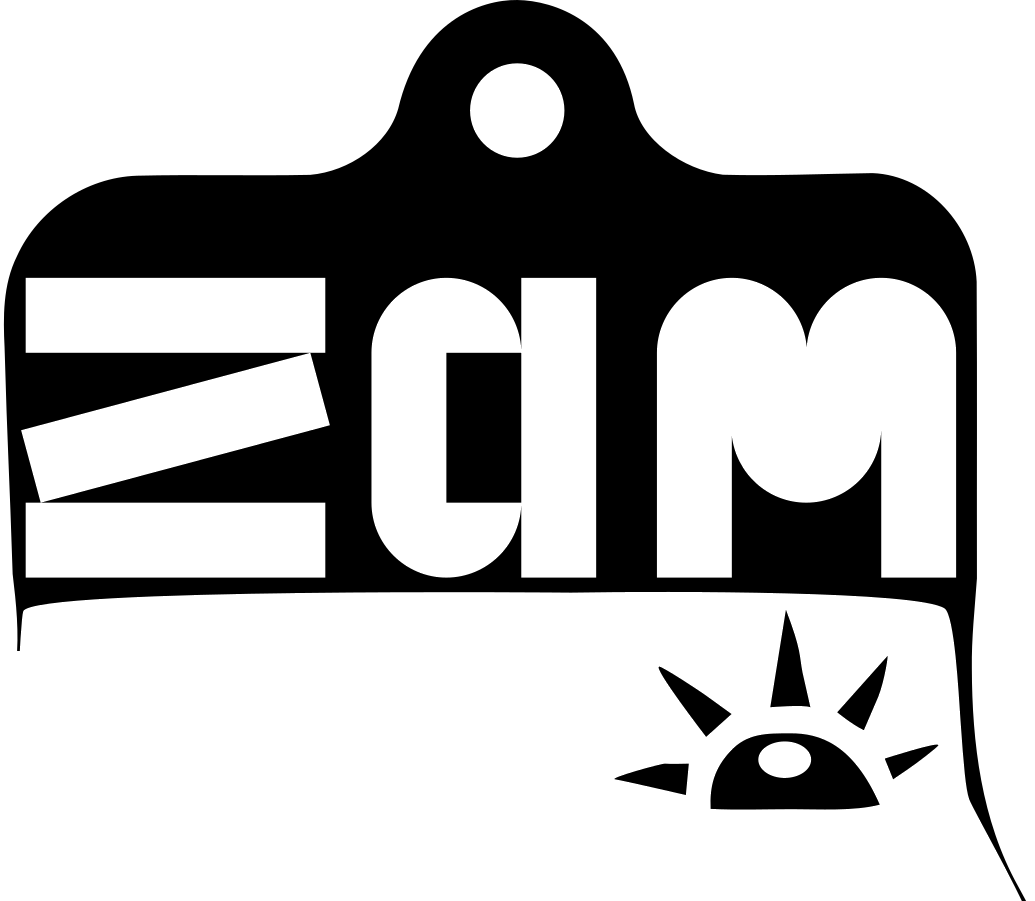
Tag 2. Erstellen des Designs
Once I had KiCad available I proceeded to turn the SVG of the graphic into a PCB. To achieve this, the layer feature of Inkscape was invaluable.
 |
The original image was exported as Front Copper (F.Cu). This will ensure that the section of the board that represents the head and letters will be opaque and not letter any light through. |
 |
The next layer to export as the solder mask. For the entire image was exported but this has to be converted to a negative since this defines where the solder mask should not go. |
 |
This image is then taken into a graphics program such as GIMP or Krita and trimmed down as the entire outline for this design. |
 |
The last layer is based on the entire image and converted to an outline. This is then expanded using the Outset tool. This will ensure that milling tool following the edge cut will not conflict with the actual image outline. |
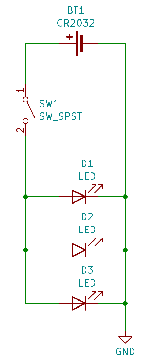
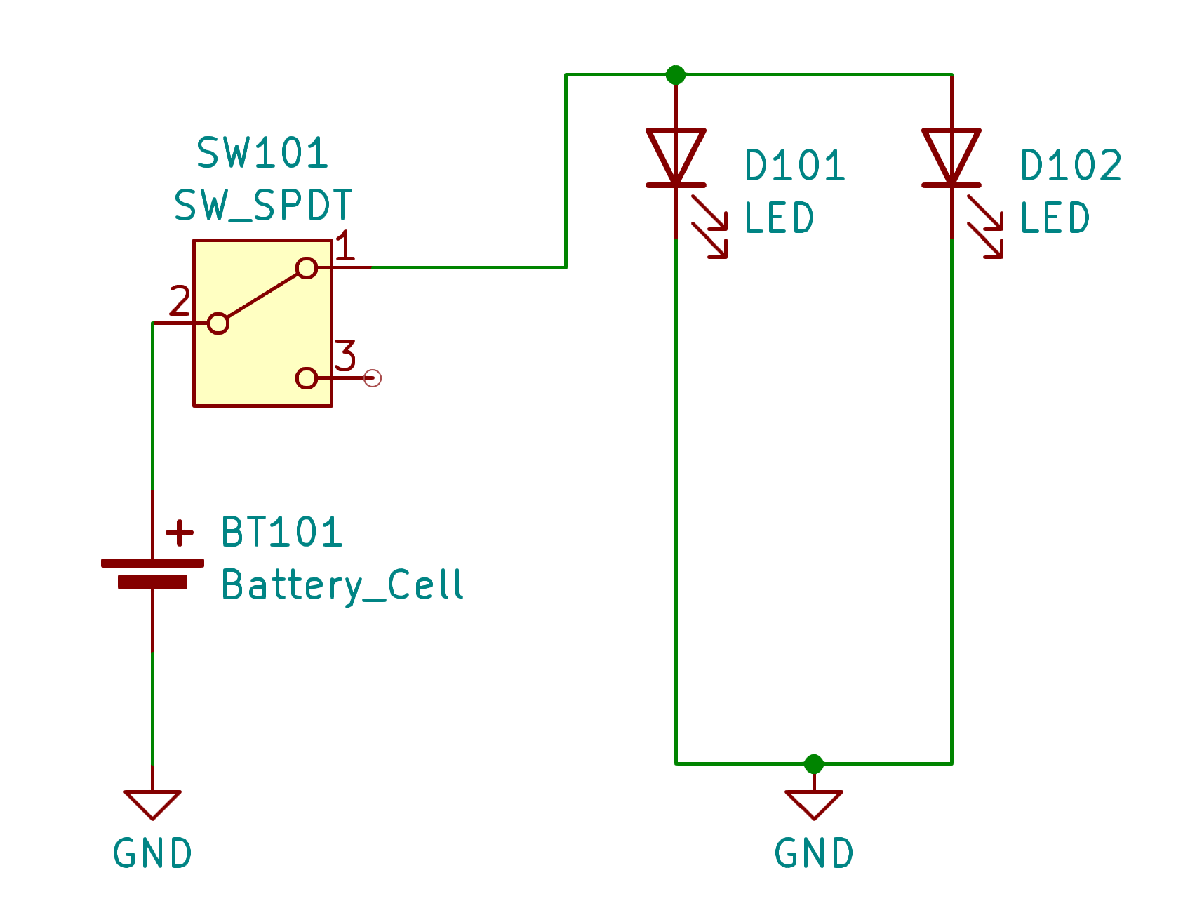
Once the layers are exported and verified, the layout of the board can begin. First of all, a simple circuit is created to defined the required parts. We don't have a lot of time for this project to try things out. So I opted to have space for three LEDs thought I believe only two will be required.

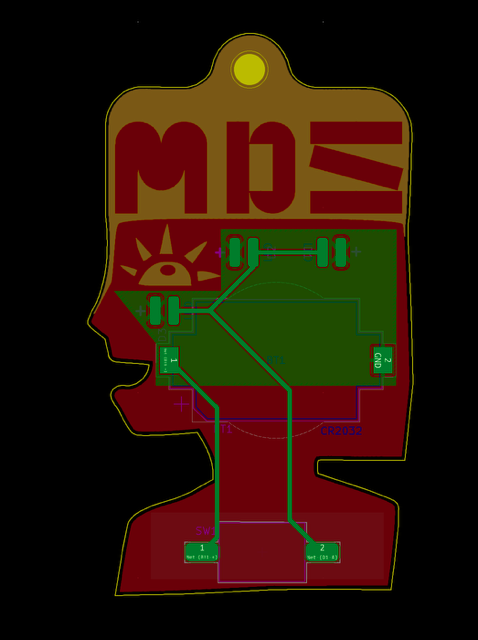

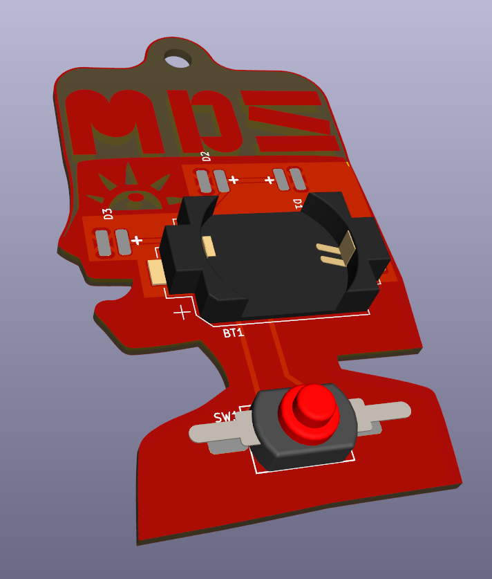
Tag 3. Montage und Prüfung
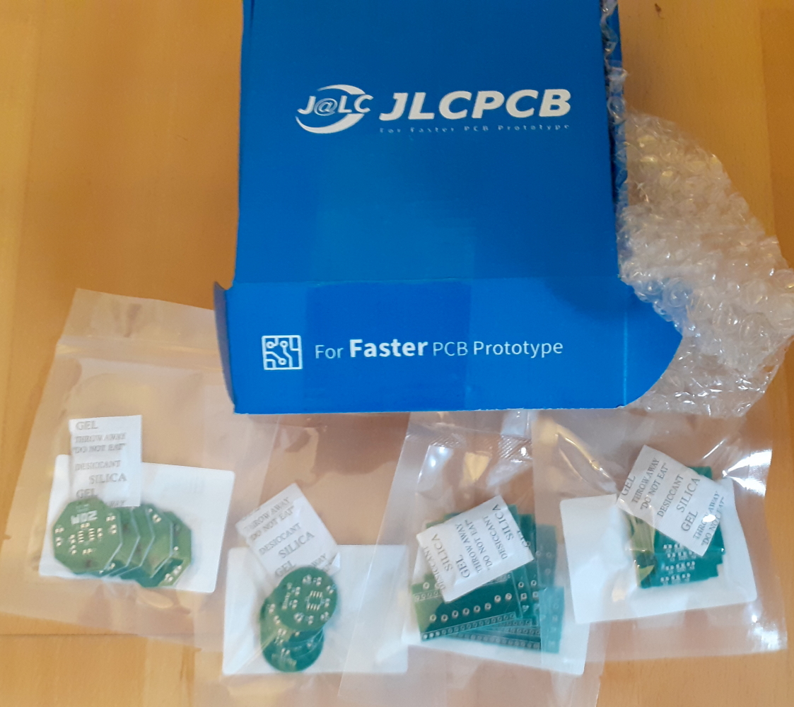
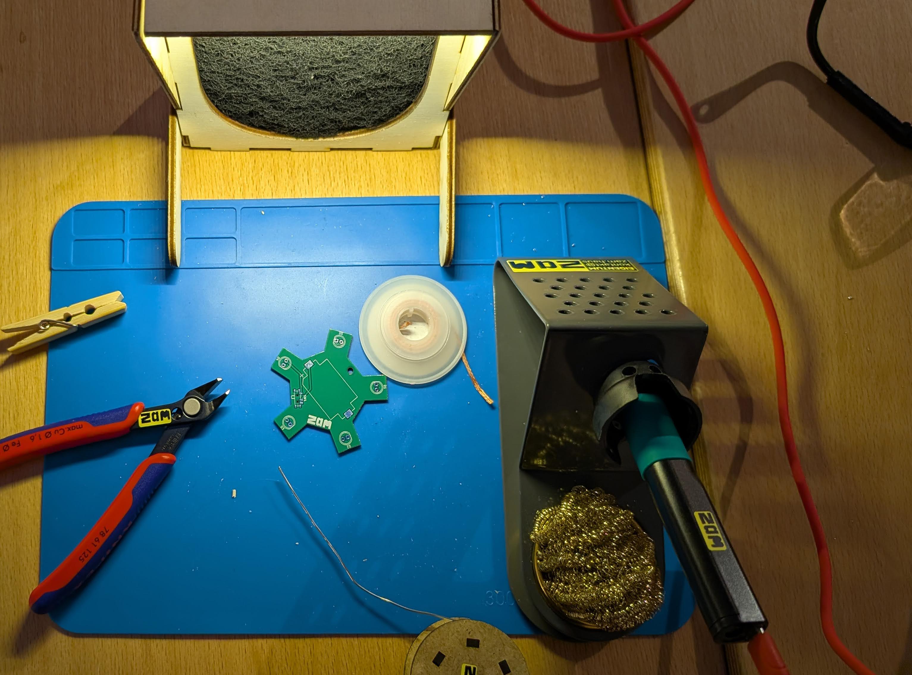
A week or so after uploading the design files to the fabricator, a panel arrived in the post. I had to assemble to see if there were any issues.
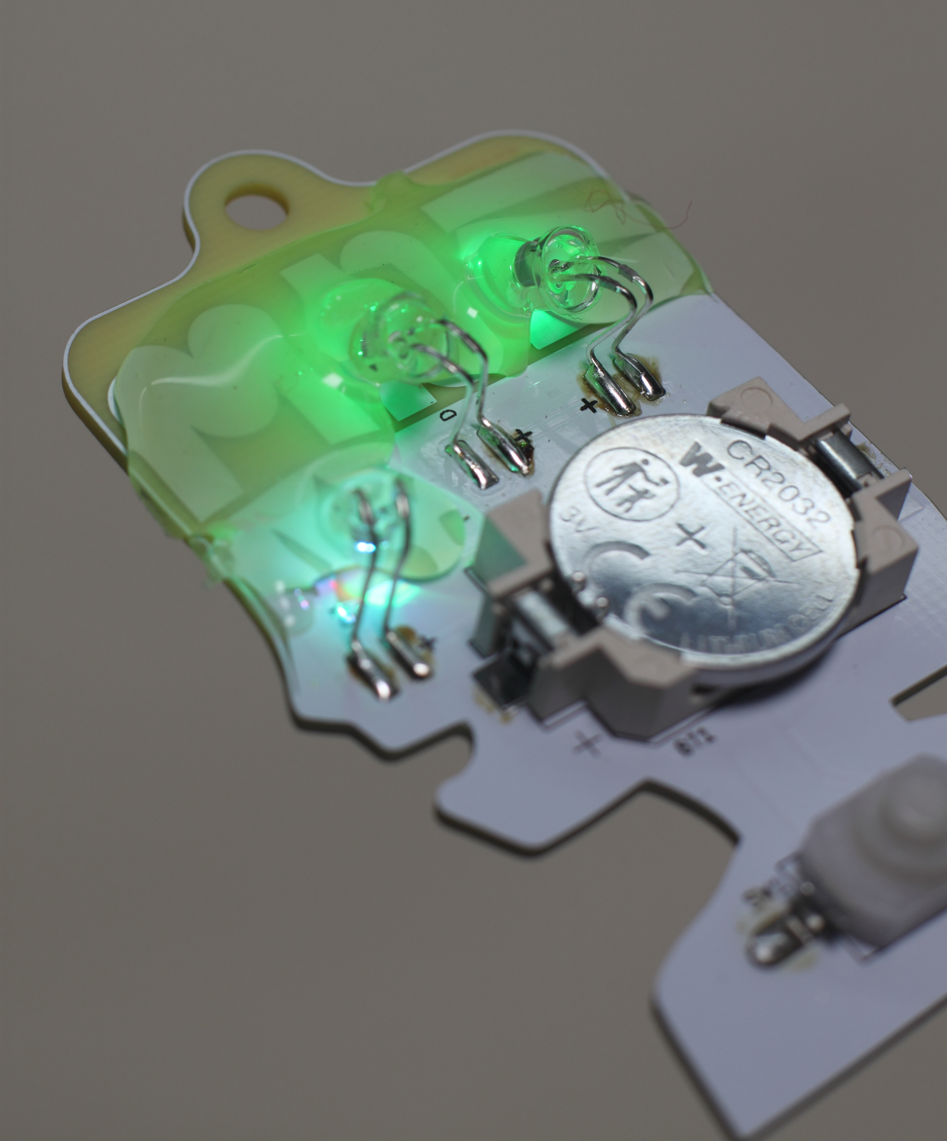
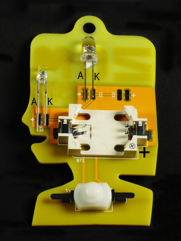
The assembly is quite simple. We start by soldering the LEDs first. The battery holder is large and the LED pads are quite close. There is a risk of damaging the battery holder if the soldering iron should touch it while soldering the LEDs.
The leads of the LEDs should be bent into place and cut to length. Make sure to take note of the anode and cathode of the LED. These leads need to connect to the appropriate pad. If they are connected the wrong way, you will not damage the LED. It just won't glow. The anode is the longer lead and should be placed on the pad marked with the plus (+) sign.
After the LEDs are soldered in place, then the battery holder and switch can be placed on the board. Like the LEDs take note of the orientation of the battery holder. Refer to the graphic below to see the correct orientation. The ⊕ marking on the battery holder should be bottom right as shown in the image.
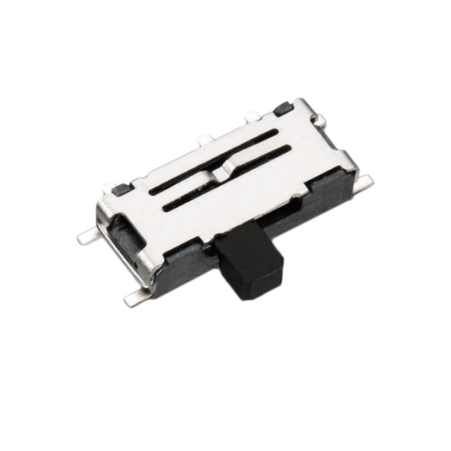
The switch has no special orientation. The leads will need to be bent into shape so that they neatly touch their pads.
Note that for the battery holder and the switch you might need to apply more heat to get a good connection.
Bauteile
- 3mm LED - eye
- 5mm LED - ZAM letters
- CR2032 Knopfzellhalter
- Schalter
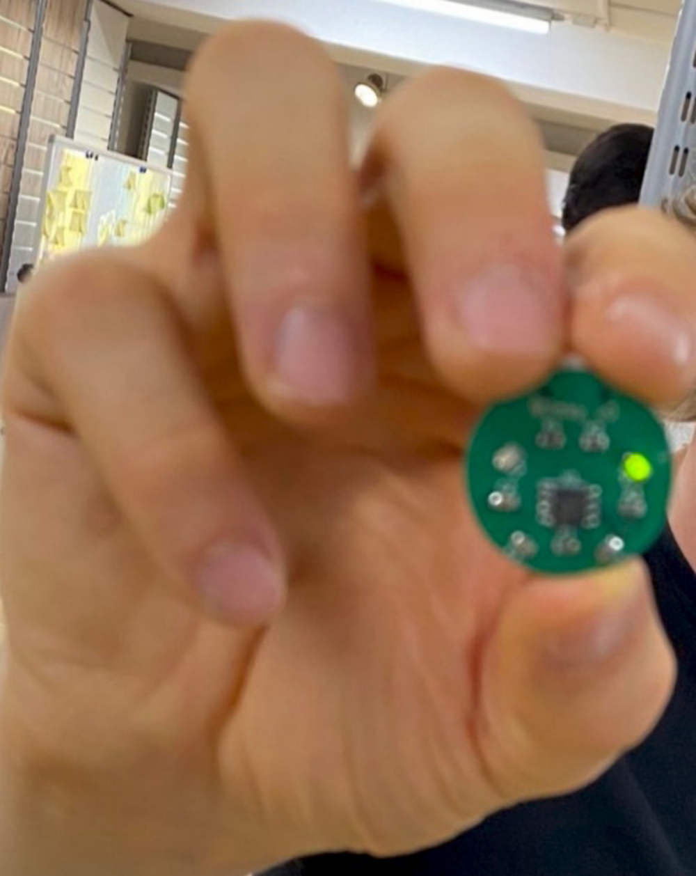
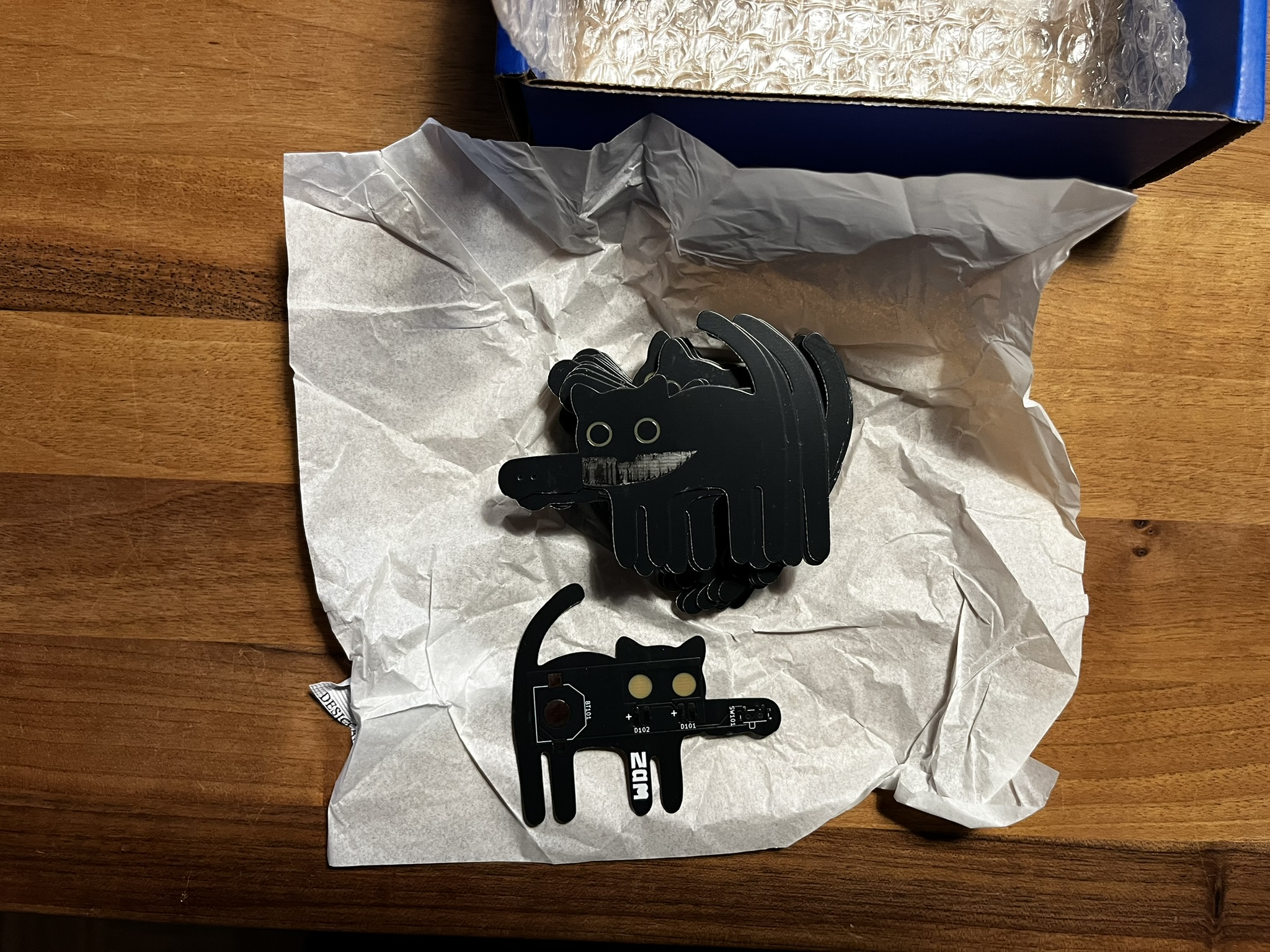
ZAM Badge - Cat with Knife
Überblick
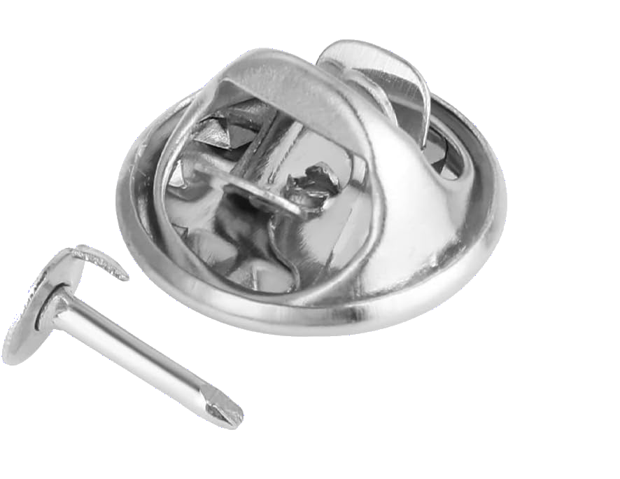
Schumi thought it would be cool to have a badge available for Wintergalaktische Club-Mate Party 2025 (WCPM). The design would be based on a Cat with Knife pin.
[Photo of the original pin]
Projekt-Metadaten
Cat with Knife GitHub Repository
Schumi daniela.novac@betreiberverein.de
Steve Mayze smayze@yahoo.com
Logbuch / Schritte
Tag 1 Friday 07.02.2025
We discussed the design
[PHOTO of the model badge]
Tag 2 Saturday 08.02.2025
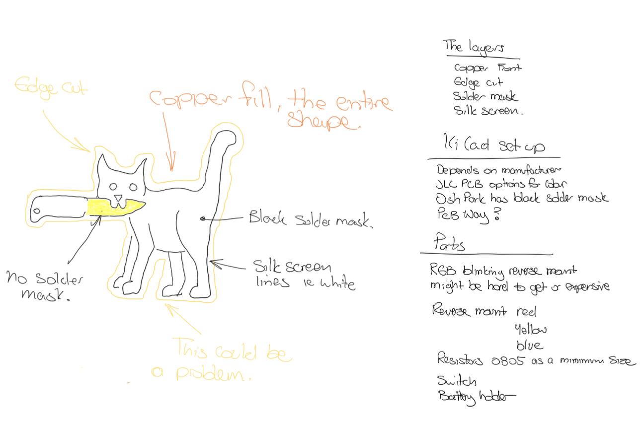
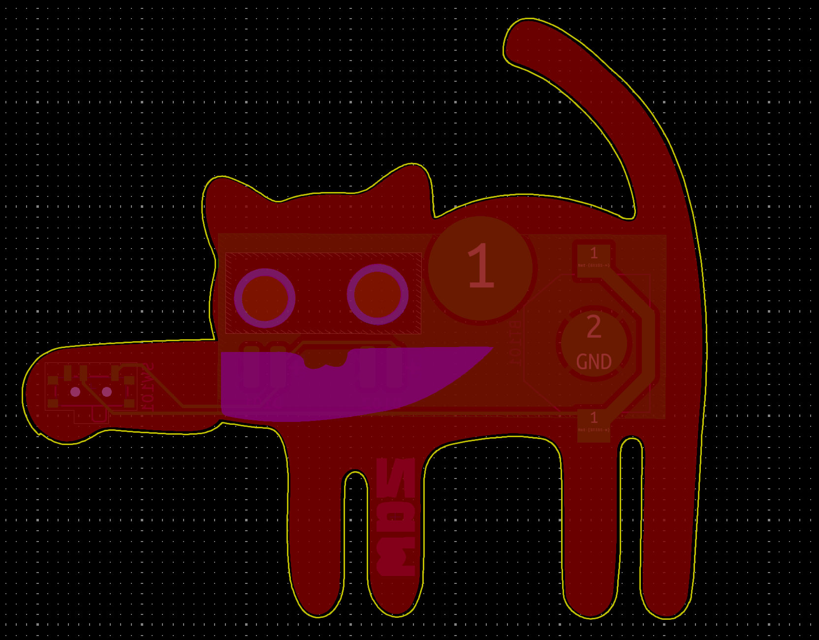
A PCB is made up of layers. These layers can be set up to create images by capitalising on the shading effect of each layer. This project was relatively simple in that the bulk of the form was one colour. The only special requirements were with the eyes and the knife blade.
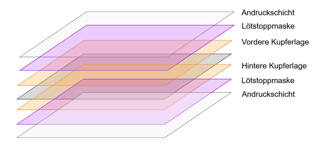
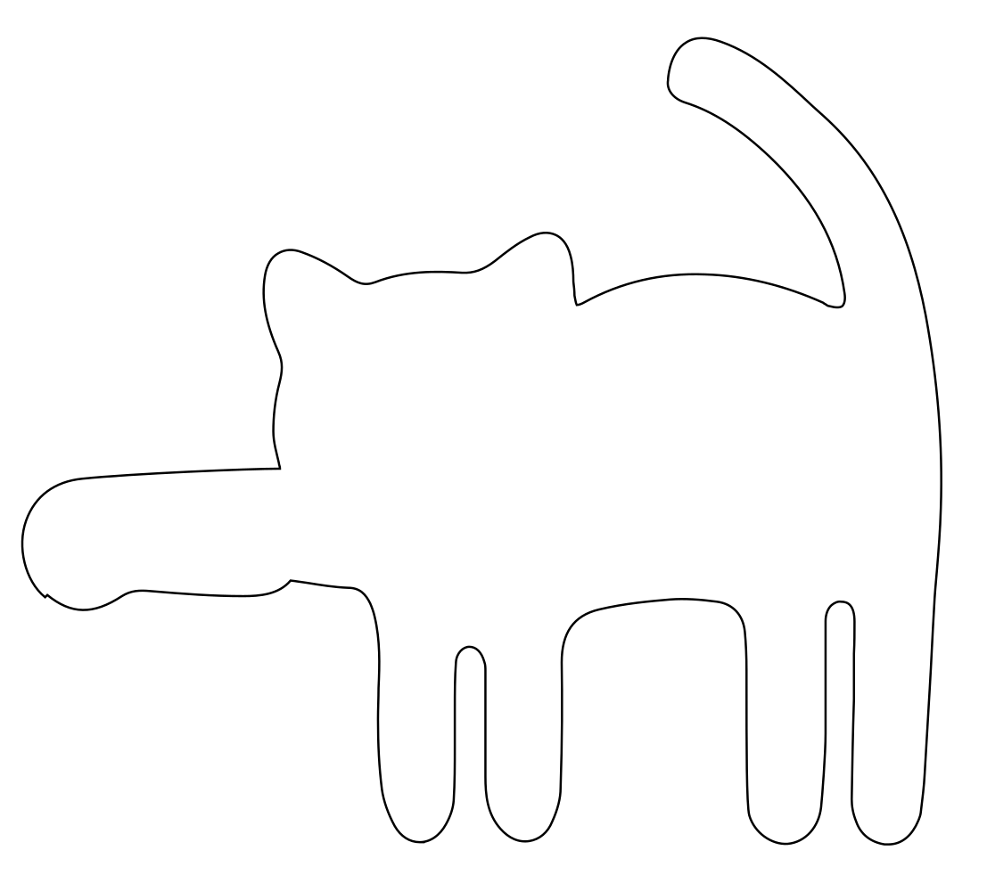
For any board the first thing to define is the edge-cut. This layer of the design defines the outside boundary of the board. Ideally this needs to be 0.5mm bigger than the actual image itself as this will define the path that the cutting tool will make to create the board shape. If the edge cut is too close to the actual outline of the image, then parts of the image could be cut off.
In the sketch below Steve put together some initial ideas on how he believed the layers could stack up.
Tag 3. 11.02.2025
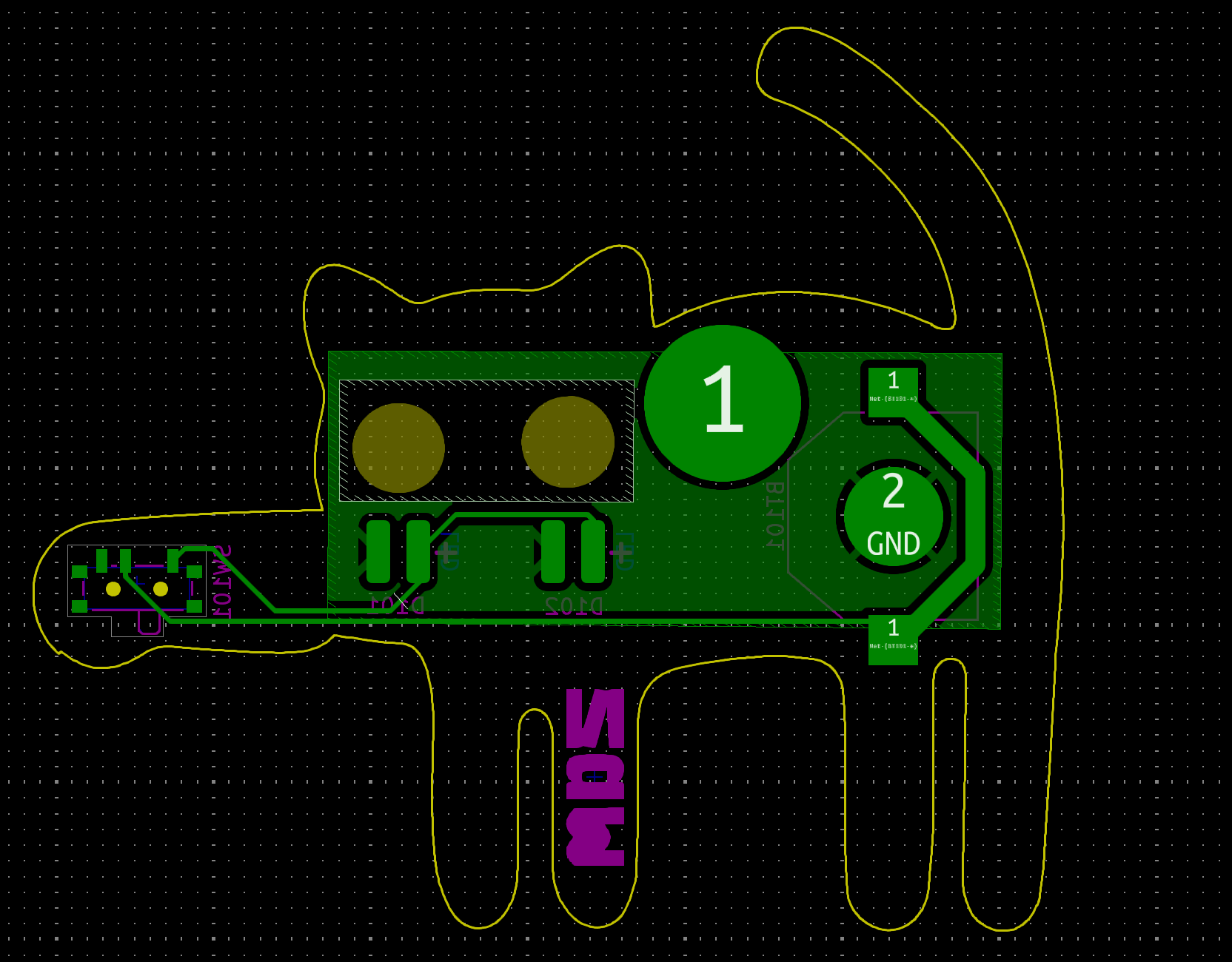
Schumi created the graphic files required - Edge Cut, Front Copper, Solder Mask, Back Solder Mask. There was a bit of going back and forth between Illustrator and KiCad to ensure that we could create the desired effect. Rather than having the eyes as glowing discs, the intention is to have the eyes as glowing circles. To achieve this we needed to ensure that there was neither copper nor solder mask on both the front and back of the board where the eyes are. This then exposes the underlying, translucent substrate layer. This effect could be created by modelling the eyes in the front copper layer as shown in the image below.
|
|
|
| Edge Cut | Front Copper |

The above copper layer is not enough. We need to be sure that the black solder mask would not cover the eyes nor the knife blade. When designing a PCB, the font solder mask (the image below left) defines where the solder mask should not be applied. This ensures that the board substrate layer will be visible around the eyes and that the copper is exposed for the knife blade. During fabrication, the exposed copper will be coated with a solder layer. This will render the knife blade silver in colour.
The back solder mask (the image below right) also defines where there is no solder mask. The PCB design will ensure that there is no copper also at this position, exposing the underlying board substrate. This then will enable light from the LEDs to shine through the translucent substrate.
|
|
|
| Front Solder Mask | Back Solder Mask |


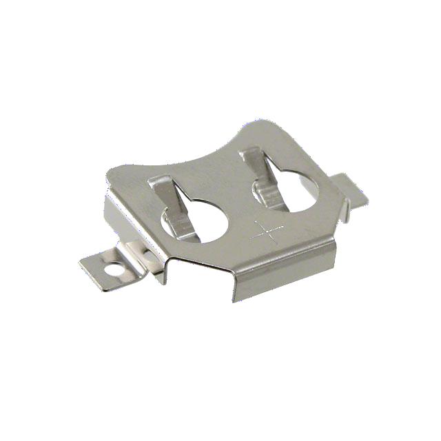
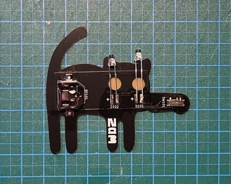
A decision needed to be made as to the size of the board. It is a two way decision - The size of the board can dictate what parts to choose based on their size but also the requirements of the project can be that certain parts are unavoidable so the board must be big enough to accommodate these parts. In our case, it was thought to use reverse mounted LEDs This would not have been a problem but a further requirement was for blinking LEDs. The sourcing self blinking reverse mounted LEDs was problematic. It could have been possible with more electronics but time constraints meant we needed a simpler solution. It was decided to use 3mm self blinking LEDs, that could be bent into position behind the eyes. The next problem was the power source. This would also be the largest part on the board. The smaller holder for the battery series CR 1216, 1220 and 1225 was chosen. Along side the smaller battery holder, a small slide switch was chosen. Using self blinking LEDs with such a small battery cell makes the design relatively simple. i.e. there is no need to provide any current limiting resistors.
 |
 |
 |
An additional place was made on the board to be able solder on a butterfly-pin so that the badge could be easily fixed to clothing.
|
|
|
| PCB design with front copper pour | PCB design without the front copper pour, showing the back copper. |
|
|
|
| 3D view of the final design |
3d view of the back side of the PCB |


The design files were sent off for fabrication, selecting a board thickness of 0.8mm to maximise the amount of light able to shine through and a black solder mask to match the original badge colour.

Tag 4. 28.02.2025
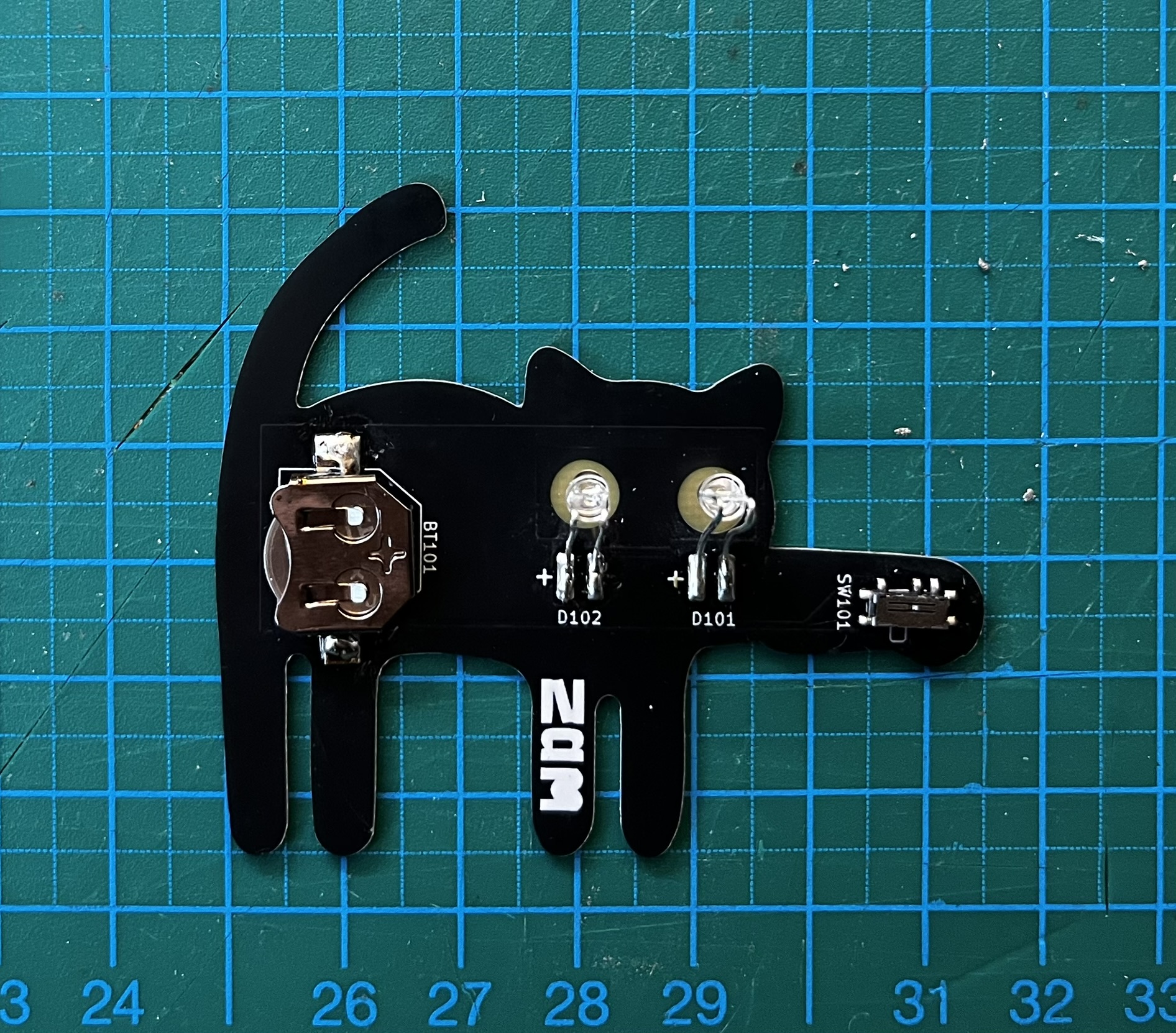
The boards arrived so they were unpacked immediately and one was assembled to see if there were any issues.
 |
 |
| For this build, 3mm slow blinking LEDs were chosen. Equally, any though-hold LED can be used. |
It was noted that the pad intended for the butterfly pin was omitted from the board but it is definitely in the design files. There was not notification that Steve was aware of for the fabrication to omit this. Probably on the grounds that there was no electrical connection and that it was only a place holder and not a real part
It was discovered during assembly that the large round pad for the battery should be tinned with some solder. This will ensure that the contact is raised above the solder mask. Otherwise the battery will not be able to make a good contact.
 |
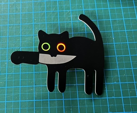 |
| The assembled parts with the LEDs bent into position |
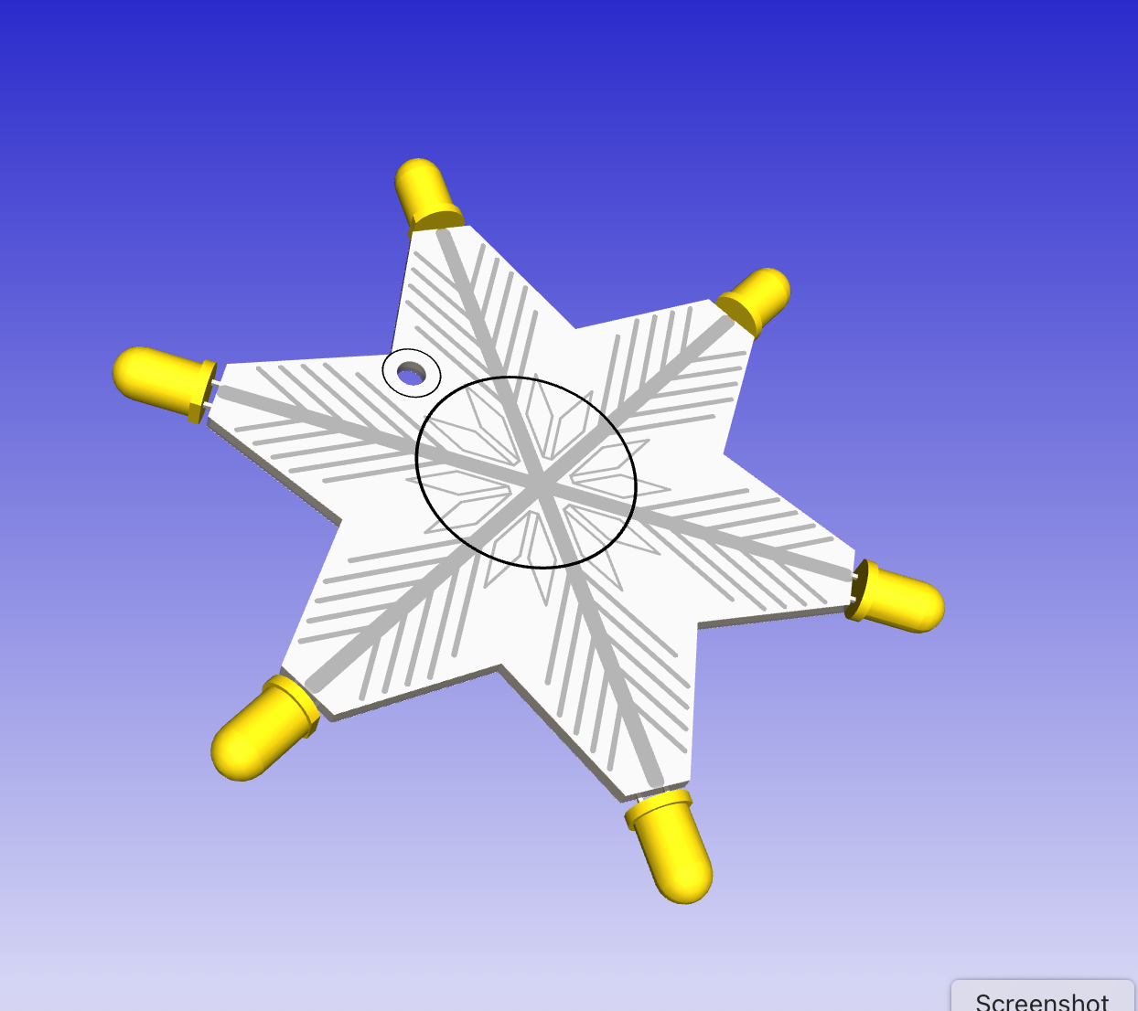
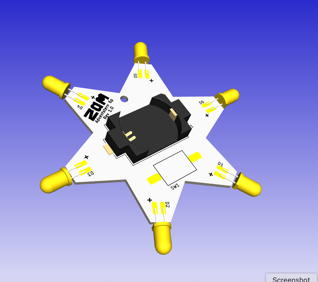
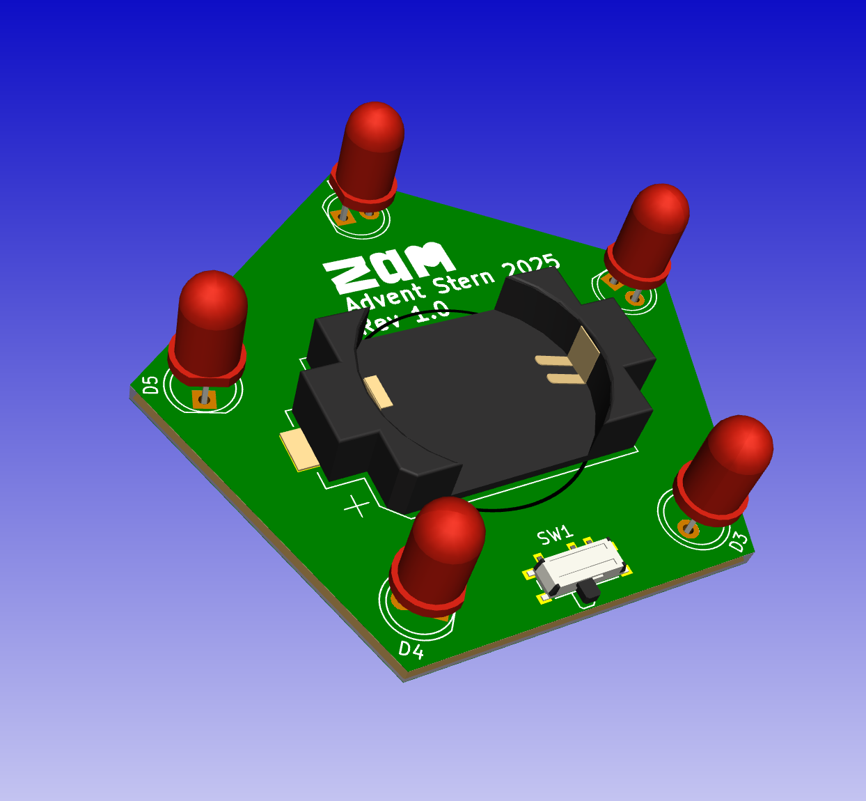
Advent Löt-Aktion - Sternen
|
Motivation / Grundidee |
Im Rahmen einer öffentlichen Vorweihnachtsveranstaltung im offenen Werkraum ZAM wurden Familien und insbesondere Kinder eingeladen, gemeinsam kreative Aktivitäten rund um die Advents- und Weihnachtszeit durchzuführen. Ein Schwerpunkt lag dabei auf dem Basteln und Gestalten von Sternen als adventliche Dekoration. Vor diesem Hintergrund entstand der Wunsch nach einer einfachen, kindgerechten Einführung in das Löten. Ziel war es, Leiterplatten (PCBs) zu entwerfen, die thematisch zum Advent passen, robust genug für Anfänger:innen sind und gleichzeitig einen sichtbaren, motivierenden Erfolg bieten. Analog zum bereits bekannten ZAM Badge 2024 sollten die Platinen als eigenständige Lötübungen dienen. Das Ergebnis sind zwei Stern-PCB-Designs (fünf- und sechszackig), die mit blinkenden LEDs bestückt werden und nach dem Löten als leuchtende Adventssterne genutzt werden können. |
|
Platzbedarf |
Für die Durchführung der Advent-Löt-Aktion wird kein dauerhafter Platz benötigt. Die Aktivität kann an vorhandenen Werkbänken im ZAM durchgeführt werden. Benötigt werden pro Arbeitsplatz:
|
|
Ab wann / wie lange |
Die eigentliche Lötübung pro Stern dauert – je nach Erfahrung – etwa 15–30 Minuten. |
|
Kontakt |
Name: Steve Mayze @smayze Projekt: ZAM Advent Star GitHub: https://github.com/SteveMayze/ZAM-Advent-Star |
Projekt-Metadaten
Geräte & Werkzeuge
-
Lötstation (temperaturgeregelt)
-
Lötkolbenständer mit Schwamm
-
Elektronik-Lötzinn
-
Seitenschneider
-
Dunstabzug
Materialien
-
Leiterplatten (5-zackiger Stern und 6-zackiger Stern)
- Rote blinkende LEDs - 5-zackiger Stern
-
Weiße blinkende LEDs - 6-zackiger Stern
-
Batterie (z. B. CR2032 oder vergleichbar)
-
Batteriefassung
-
Ein/Aus-Schalter
Zeitaufwand
-
Konzept & Design: ca. 2–3 Tage (iterativ)
-
PCB-Layout & Prüfung: ca. 2–3 Tage
-
Fertigung & Lieferung: ca. 1–2 Wochen (extern)
-
Lötübung pro Stern: ca. 15–30 Minuten
Design Files
GitHub Repository
Alle Design-Dateien (KiCad), Produktionsdaten und Dokumentation befinden sich im GitHub-Repository:
https://github.com/SteveMayze/ZAM-Advent-Star
Enthaltene Projekte:
-
ZAM-AdventStar-Small – fünfzackiger Stern
-
ZAM-AdventStar-SixPoint – sechszackiger Stern mit Eiskristall-Design
Design-Varianten
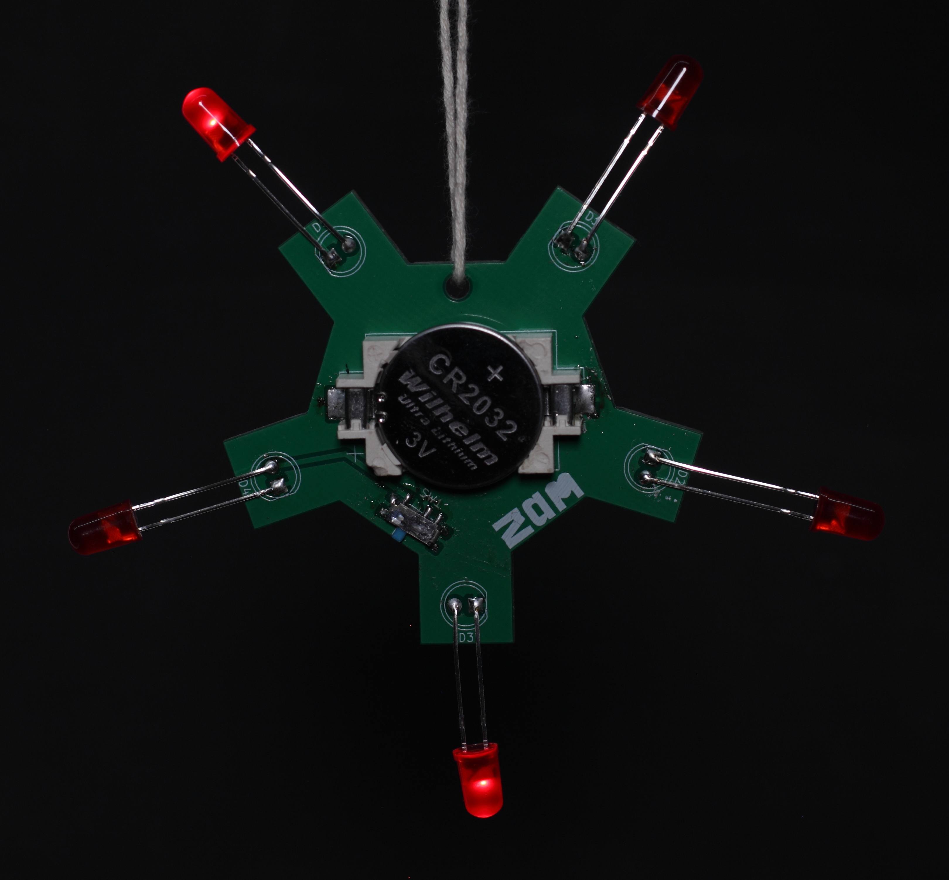
5-zackiger Stern (Small)
Ausgehend von einer einfachen Pentagon-Form wurde ein fünfzackiger Stern entworfen, bei dem die Spitzen ausgespart sind. An diesen Positionen werden weiße oder roter, blinkende LEDs eingelötet. Die LEDs können leicht nach außen gebogen werden, wodurch eine plastische Sternform entsteht.
Merkmale:
-
einfache Geometrie
-
gut geeignet für jüngere Kinder
-
Batterie und Schalter direkt auf der Platine
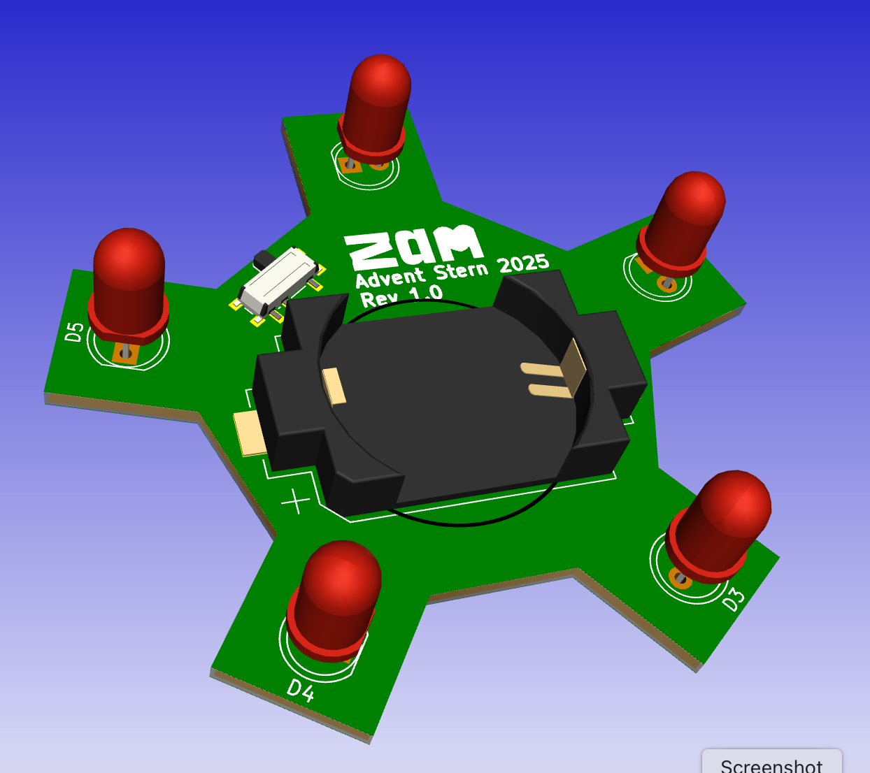
Erweiterbarkeit / kreative Weiterverwendung:
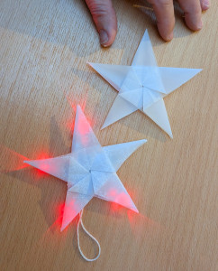
Durch das sehr kompakte und einfache Design eignet sich der 5-zackige Stern besonders gut als Lichtquelle für andere Stern- und Bastelprojekte. Ein Beispiel ist die Montage der Platine auf der Rückseite eines gefalteten Origami-Sterns aus transluzentem Bastelpapier. Das Papier streut das Licht der LEDs weich und erzeugt einen dekorativen Leuchteffekt.
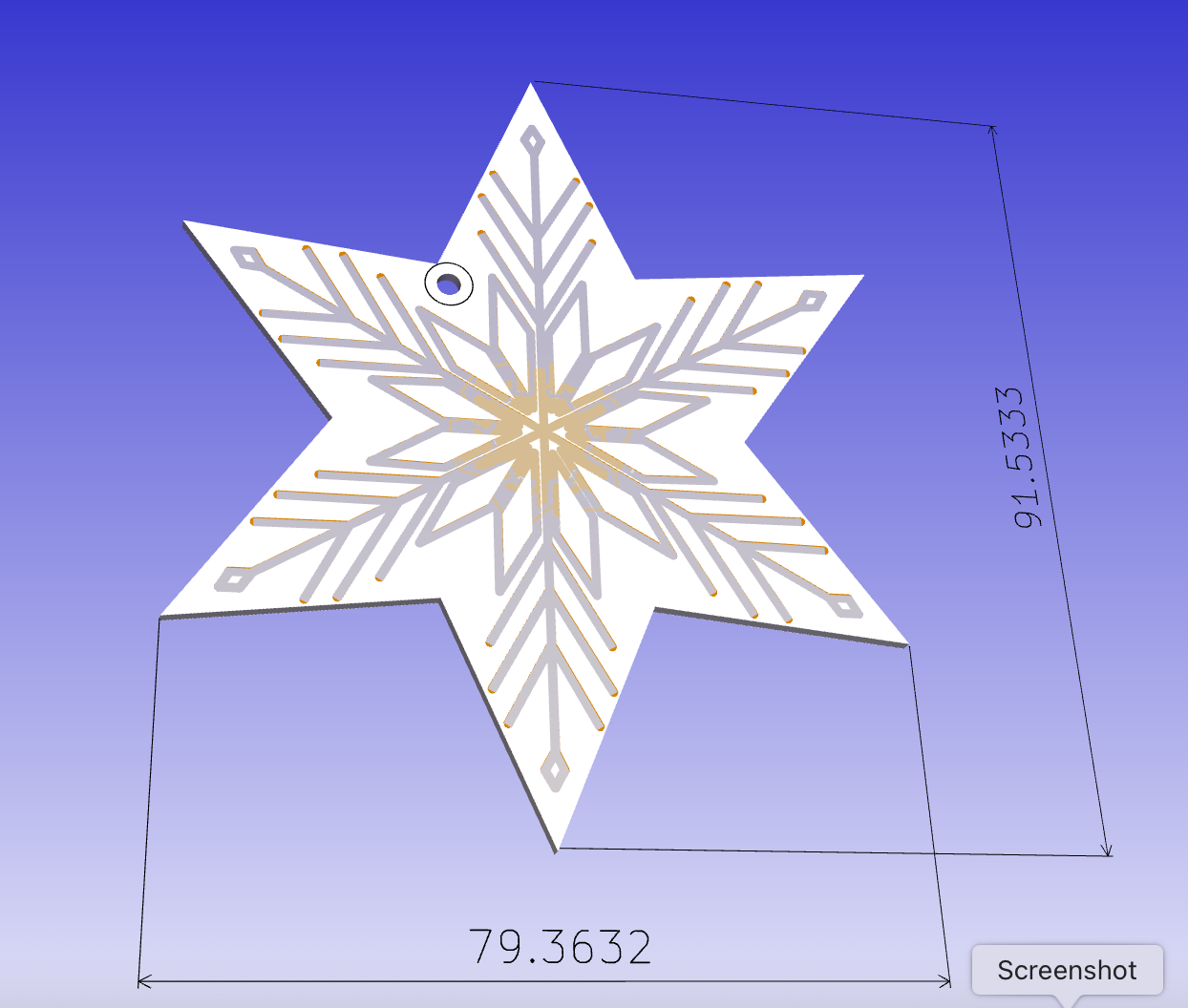
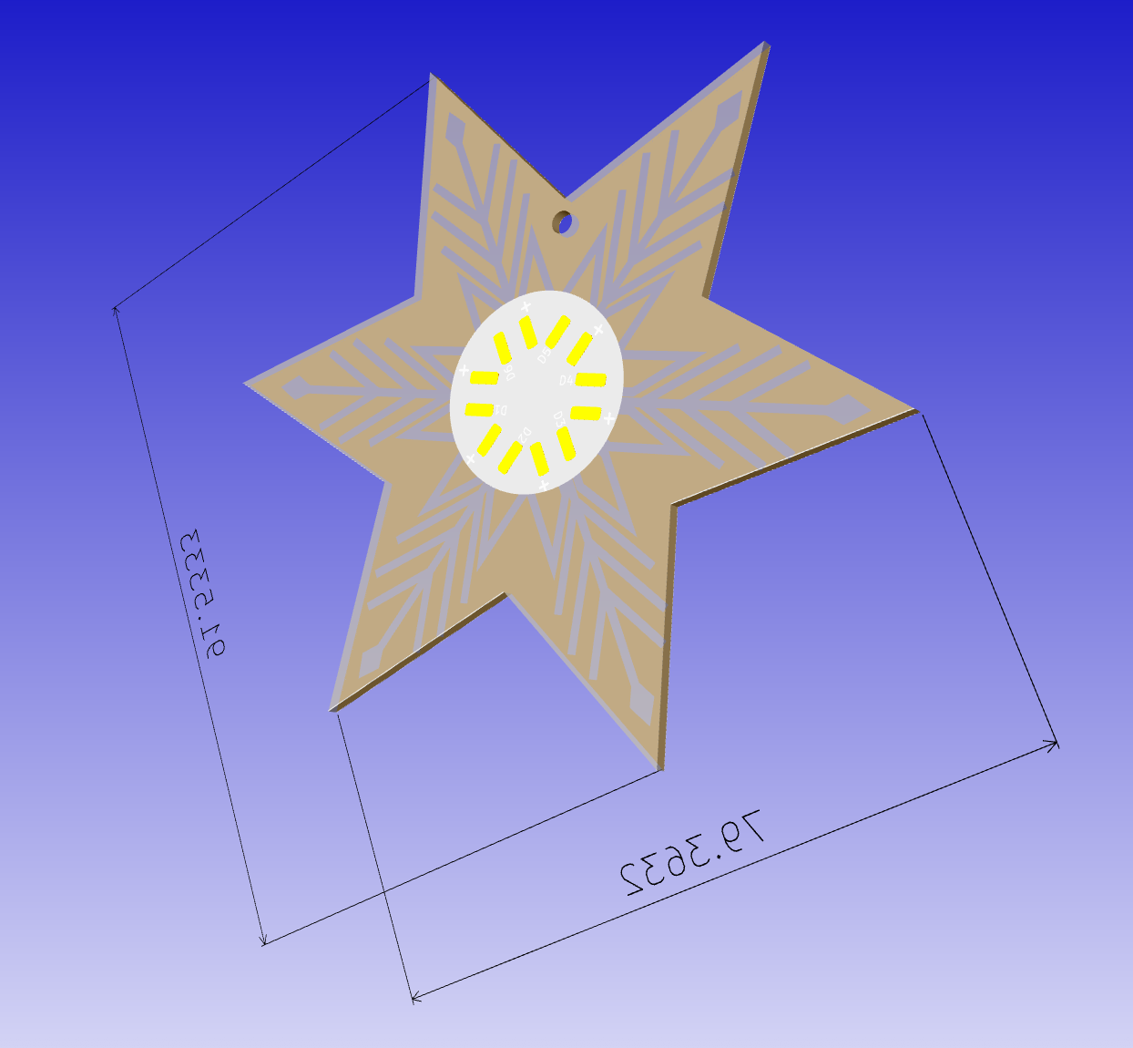
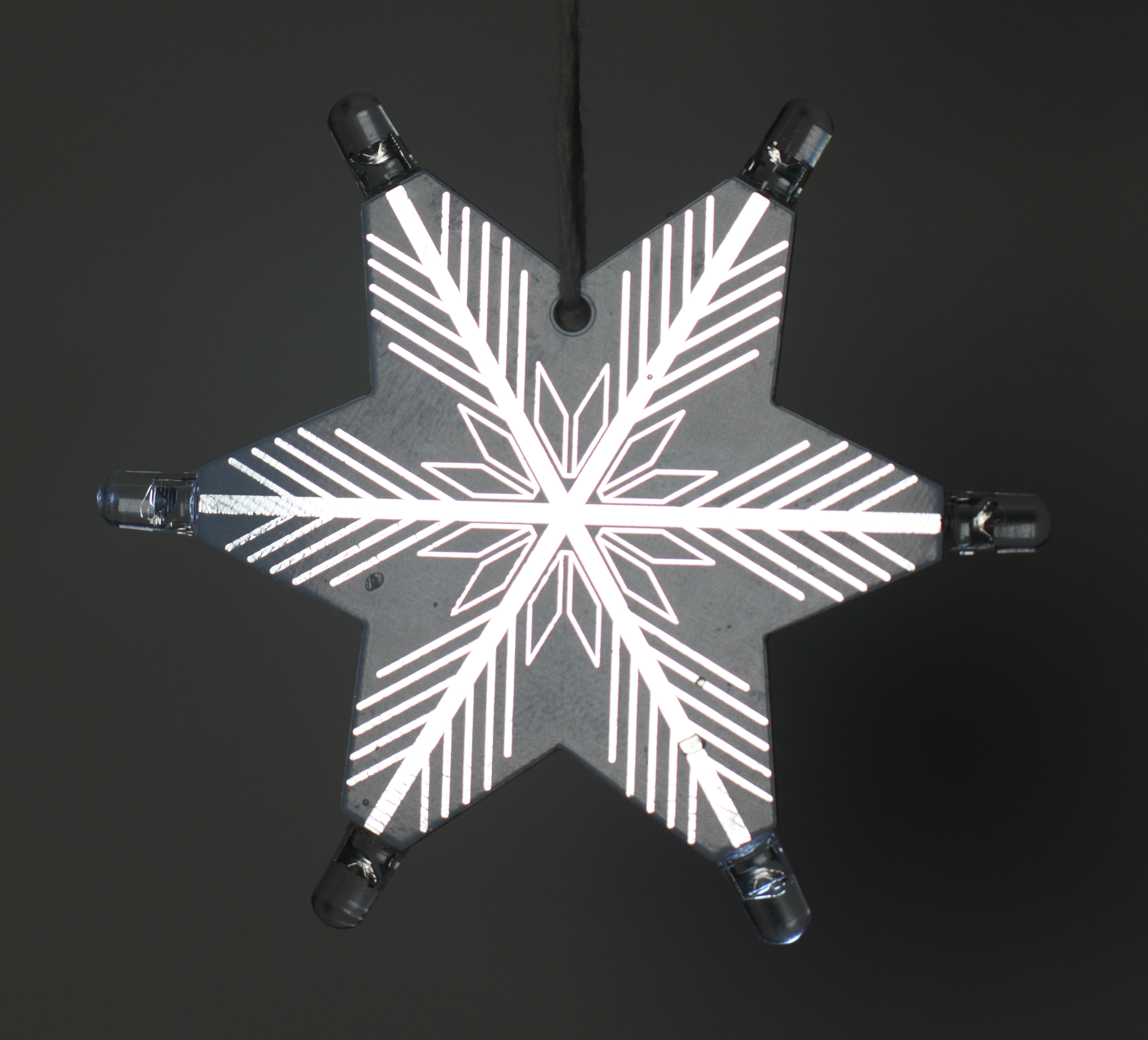
6-zackiger Stern – „Ice Crystal“
Dieses Design kombiniert die Sternform mit einem Eiskristall-Motiv. Die kristalline Struktur ist als freiliegendes, verzinntes Kupfer ausgeführt und reflektiert das Umgebungslicht. Anders als bei der ursprünglichen Idee wird das Licht nicht von hinten durch die Platine geführt, sondern über die an den Spitzen angebrachten weißen Blink-LEDs erzeugt.
Merkmale:
-
sechszackige Sternform
-
dekoratives Eiskristall-Muster aus Kupfer
-
visuell hochwertig, auch ohne aktive Beleuchtung
 |
 |
Montageanleitung (Bausatz)
Die folgenden Schritte beschreiben die empfohlene Reihenfolge für den Zusammenbau der Advent-Stern-PCBs. Die Anleitung ist bewusst einfach gehalten und eignet sich auch für Lötanfänger:innen und Kinder (mit Aufsicht).
1. Schalter anbringen
Der Ein/Aus-Schalter wird auf der Vorderseite der Platine nahe am Rand angebracht.
-
(6-zakige Stern) Die Pins des Schalters ggf. leicht biegen, sodass sie gut auf den Lötpads aufliegen.
-
Die beiden Lötpads auf der Platine leicht vorverzinnen.
-
Den Schalter auf die Pads setzen (Ausrichtung ist egal).
-
Pads und Pins gleichzeitig erhitzen, bis das Lötzinn sauber zusammenschmilzt.
2. LEDs anbringen
An den Sternspitzen werden weiße, blinkende LEDs eingesetzt.
-
Wichtig: LEDs sind polarisiert.
-
Langer Draht = Plus (+)
-
Kurzer Draht = Minus (–)
-
-
Der lange Draht muss mit dem auf der Platine markierten + übereinstimmen.
-
Die LED-Pins können leicht nach außen gebogen werden, sodass die LED optisch eine Sternspitze bildet.
-
Pins auf die Lötpads setzen und verlöten.
3. Batteriehalter auf der Rückseite anbringen
-
Die Platine umdrehen.
-
Die beiden großen rechteckigen Pads leicht vorverzinnen.
-
Die Pins des Batteriehalters ebenfalls vorverzinnen.
-
Polarität beachten: Das + auf dem Batteriehalter muss mit dem + auf der Platine übereinstimmen.
-
Batteriehalter auf die Pads setzen und das Lötzinn durch Erhitzen zusammenschmelzen.
4. Batterie einsetzen & Test
-
Die Batterie zuerst unter die leicht angehobene Feder schieben.
-
Danach vollständig in den Halter drücken.
-
Schalter einschalten → die LEDs sollten nun blinken.
Falls nichts leuchtet:
-
Polarität der LEDs prüfen
-
Lötstellen kontrollieren (kalte Lötstellen?)
-
Batterie richtig eingesetzt?
Logbuch / Schritte
Tag 1 – Ideen & Konzept
Ausgangspunkt war ein sehr einfaches Design: ein Pentagon mit jeweils einer LED an jeder Ecke, deren Beinchen so gebogen werden konnten, dass optisch eine Sternform entsteht. Dieses Design erwies sich jedoch als zu schlicht.
Parallel dazu entstand die Idee eines sechszackigen Sterns mit einem Eiskristall-Motiv. Die erste Version setzte auf eine weiße Lötstoppmaske und kupferfreie Flächen, um ein Durchleuchten von hinten zu ermöglichen. Dieses Konzept wurde verworfen, da kein Platz für Batterie und Schalter vorhanden war und eine externe Stromversorgung nötig gewesen wäre.
 |
 |
Tag 2 – PCB-Design
Basierend auf den Erkenntnissen aus der Konzeptphase wurde das Fünfstern-Design überarbeitet: Die Spitzen wurden entfernt und durch LED-Lötpads ersetzt. Dieses Prinzip wurde anschließend auf den sechszackigen Stern übertragen und mit dem Eiskristall-Motiv kombiniert.
Das finale Design bietet:
-
Platz für Batterie und Schalter
-
ausreichend große Pads für Anfänger:innen
-
klare, symmetrische Formen
|
|
Tag 3 – Fertigung & Lötaktion
Nach der PCB-Fertigung wurden die Stern-Platinen im Rahmen der Adventsaktion gemeinsam mit den Besucher:innen gelötet. Beide Varianten wurden sehr gut angenommen. Besonders die blinkenden LEDs sorgten für Begeisterung bei Kindern.
 |
|
 |
 |
Fazit
Die Advent-Löt-Aktion war ein voller Erfolg. Die Kombination aus einfachem Elektronikprojekt, weihnachtlicher Gestaltung und einem sichtbaren Endergebnis hat sich bewährt. Die Stern-PCBs eignen sich hervorragend als niedrigschwelliger Einstieg ins Löten und können auch bei zukünftigen Workshops oder Veranstaltungen wiederverwendet werden.
ZAM Badge Löt-Bausäts
|
Motivation / Grundidee |
Das ZAM Badge Soldering Kit ist ein einfaches Löt-Kit, das bei ZAM-Events, Workshops und offenen Tagen eingesetzt werden kann. Auslöser für das Projekt war der Wunsch nach:
Das Kit basiert auf dem bestehenden ZAM Badge 2024 PCB Für das Soldering Kit wird dieses Design so aufbereitet, dass:
Bestandteile des Kits:
|
|
Platzbedarf |
Für die Herstellung der Kits:
Für den Einsatz bei Events / Workshops:
|
|
Ab wann / wie lange |
Projektstart: bereits erfolgt (basierend auf ZAM Badge 2024) Geplanter Ablauf:
Das Projekt ist laufend nutzbar und kann bei Bedarf immer wieder neu aufgelegt werden. |
|
Kontakt |
Name: Steve Mayze
Name: Jochen Hunger
Name: Britta Wachler Telefon / Mattermost: @britta.wachler
|
Projekt-Metadaten
Geräte & Werkzeuge
-
Lötstation (regelbar)
-
Lötkolben (feine Spitze empfohlen)
-
Seitenschneider
-
ggf. Entlötlitze / Entlötpumpe
-
Multimeter (optional, zur Fehlersuche)
Materialien
-
ZAM Badge PCB (Version 2024 Revision 2)
-
LEDs
- Schalter
- Batteriehalter
-
Batterie CR2032
-
Verpackungsbeutel
-
gedruckte Kurzanleitung
Zeitaufwand
-
Entwicklung / Anpassung: mehrere Iterationen
-
Kit-Zusammenstellung: wenige Minuten pro Kit
-
Löt-Workshop: ca. 10–20 Minuten pro Badge
Design Dokumenten https://github.com/SteveMayze/ZAM-Badge-24
Logbuch / Schritte
Tag 1 Design-Anpassungen & Farbkonzept
Ausgehend vom ursprünglichen ZAM Badge 2024 Design wurden erste Korrekturen und Anpassungen am PCB vorgenommen.
In diesem Zuge fiel die Entscheidung, das UV-Printing-Angebot von PCBWay zu nutzen. Dadurch können farbige, grafische Elemente direkt auf das PCB gedruckt werden, was das Badge visuell deutlich aufwertet.
Es wurden verschiedene Farbkonzepte in Betracht gezogen:
-
unterschiedliche Farben innerhalb eines einzelnen Badges
-
Farbverläufe vom „Head“-Bereich hin zur Beschriftung
Laut ZAM Styleguide müssen die Buchstaben jedoch stets in einer einheitlichen Farbe gehalten sein. Um das Design einfach, konsistent und gut reproduzierbar zu halten, wurde entschieden:
-
jedes Badge erhält genau eine Farbe
-
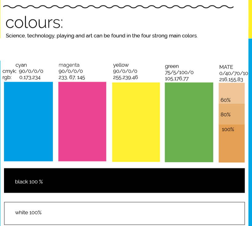
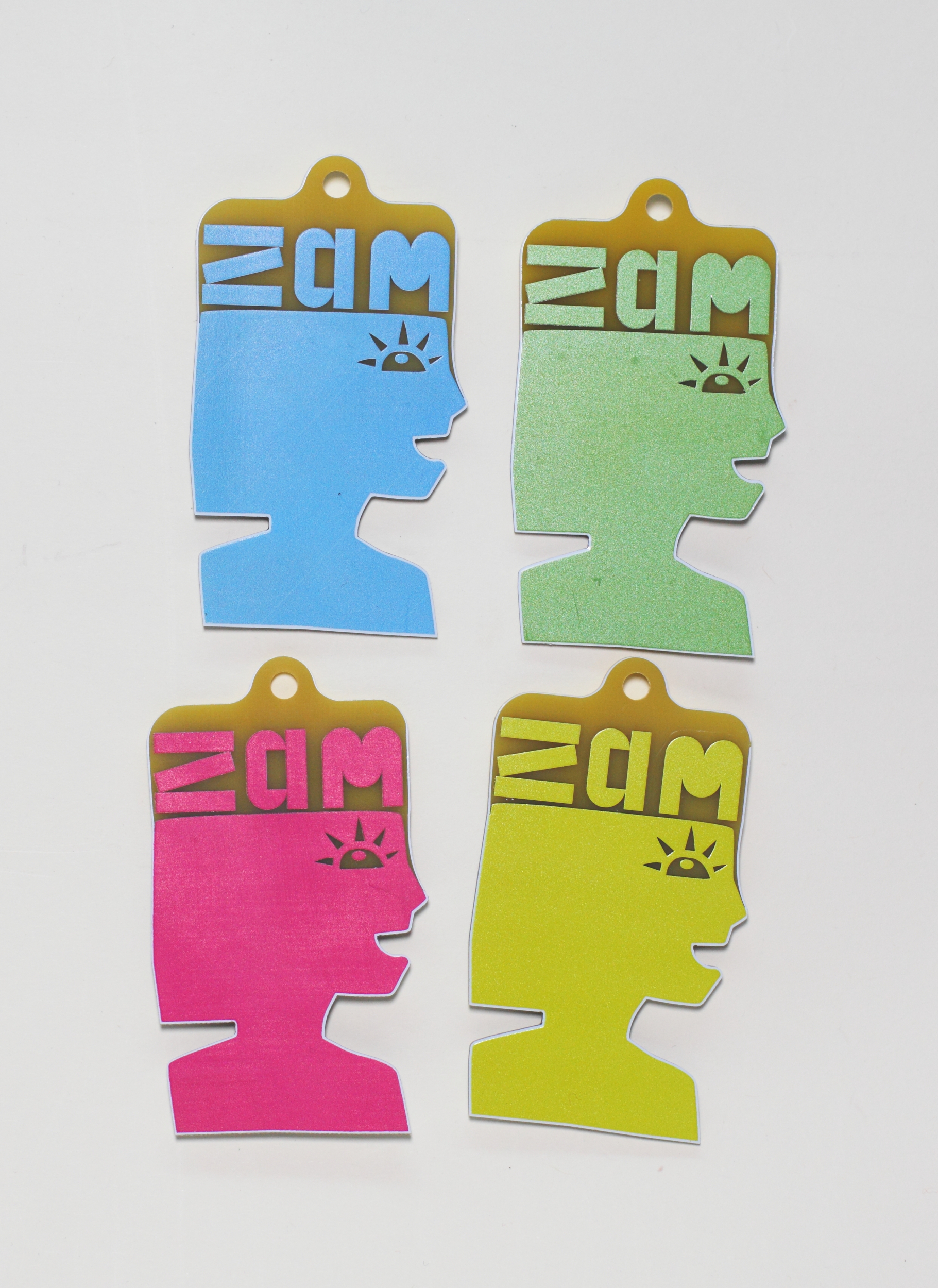
es werden vier Varianten produziert, basierend auf der offiziellen ZAM-Farbpalette
(cyan, magenta, yellow, green – siehe Grafik)
So bleibt das Design klar, CI-konform und gleichzeitig abwechslungsreich.

Tag 2 – Kit-Erweiterung & Grafikdesign
Neben dem eigentlichen Löt-Kit entstand die Idee, eine Montageanleitung zu erstellen, die gleichzeitig als Info-Flyer für das ZAM dient.
Zusätzlich wurde ein ZAM-Sticker als sinnvolle Ergänzung des Kits angedacht.
Da die grafische Gestaltung der Anleitung und des Stickers spezielle Designkenntnisse erfordert, wurde im ZAM nach Unterstützung gefragt.
Britta erklärte sich bereit, diesen Teil zu übernehmen.
Als Grundlage wurde:
-
ein Beispiel-Template für die Montageanleitung erstellt
-
das gewünschte Endformat (14 × 14 cm) definiert
-
die inhaltlichen Anforderungen (Montageschritte, kurze ZAM-Info) abgestimmt
Tag 3 – Dokumentation des Zusammenbaus
Zur Unterstützung der Montageanleitung wurde eine Fotodokumentation des Zusammenbauprozesses erstellt.
Dabei entstanden Schritt-für-Schritt-Fotos, die:
-
den Einbau der einzelnen Bauteile zeigen
-
typische Fehler vermeiden helfen
-
besonders für Anfänger*innen und Kinder geeignet sind
Diese Bilder dienen als Grundlage für:
-
die gedruckte Kurzanleitung
-
sowie eine erweiterte Dokumentation im Wiki
Bild 1–3: Vorbereitung der Bauteile
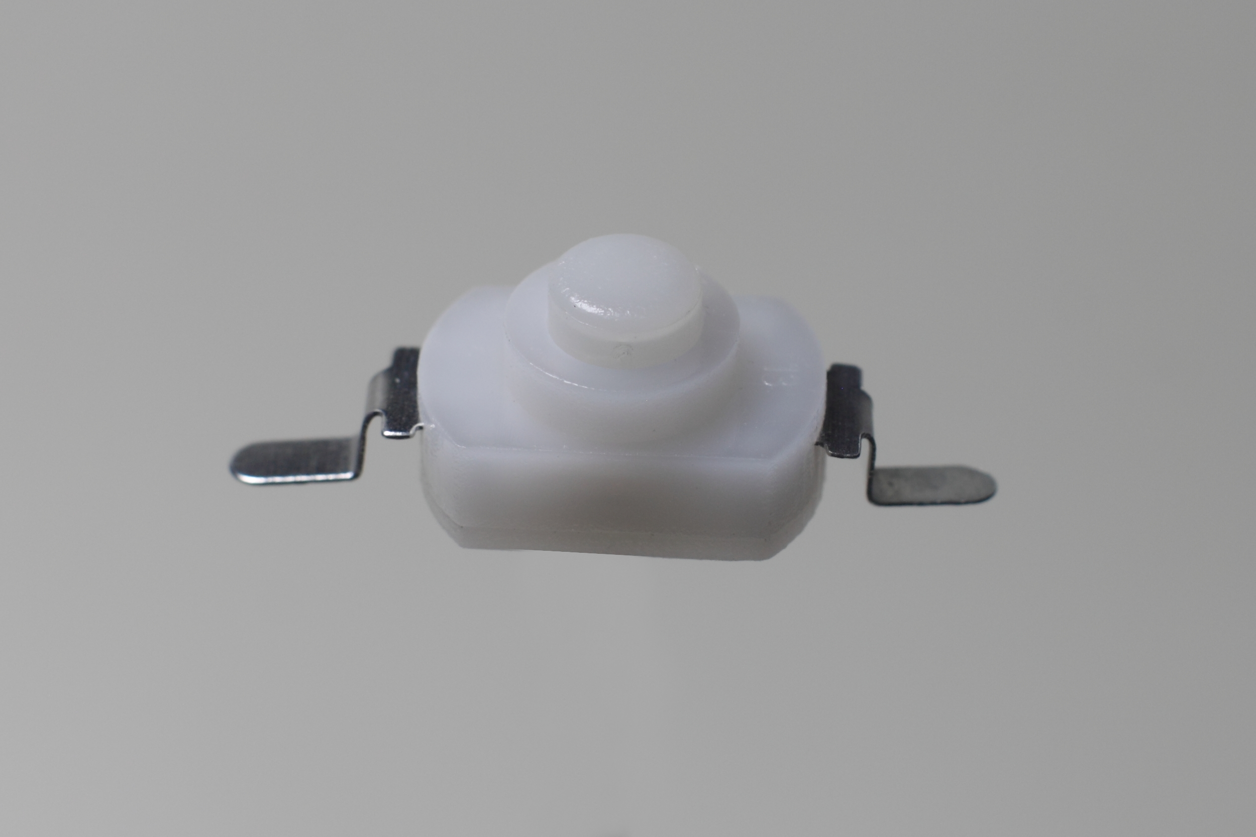
Die ersten drei Bilder zeigen das Umbiegen der Pins:
-
des Schalters
-
sowie der LEDs
Dieser Schritt erleichtert das spätere Einsetzen der Bauteile in das PCB und sorgt dafür, dass sie beim Löten plan anliegen und nicht verrutschen.
Hinweis zu den LEDs
Im ZAM Badge kommen drei LEDs zum Einsatz:
-
eine 3 mm LED für das „Auge“ des Badges
-
zwei 5 mm LEDs für die Beleuchtung der ZAM-Beschriftung
Die Anschlussdrähte (Leads) der LEDs müssen vor dem Einsetzen in die richtige Form gebogen werden, damit sie sauber in die vorgesehenen Bohrungen passen.
Dies ist deutlich einfacher, wenn es vor dem Löten erfolgt.
Für alle LEDs gilt:
-
die längere Anschlussleitung ist der Pluspol (+)
-
der Pluspol soll immer auf der rechten Seite eingesetzt werden
-
die Plus-Markierung (+) ist zusätzlich auf dem PCB aufgedruckt
Eine einheitliche Ausrichtung der LEDs ist wichtig, da sie nur in der korrekten Polung funktionieren.
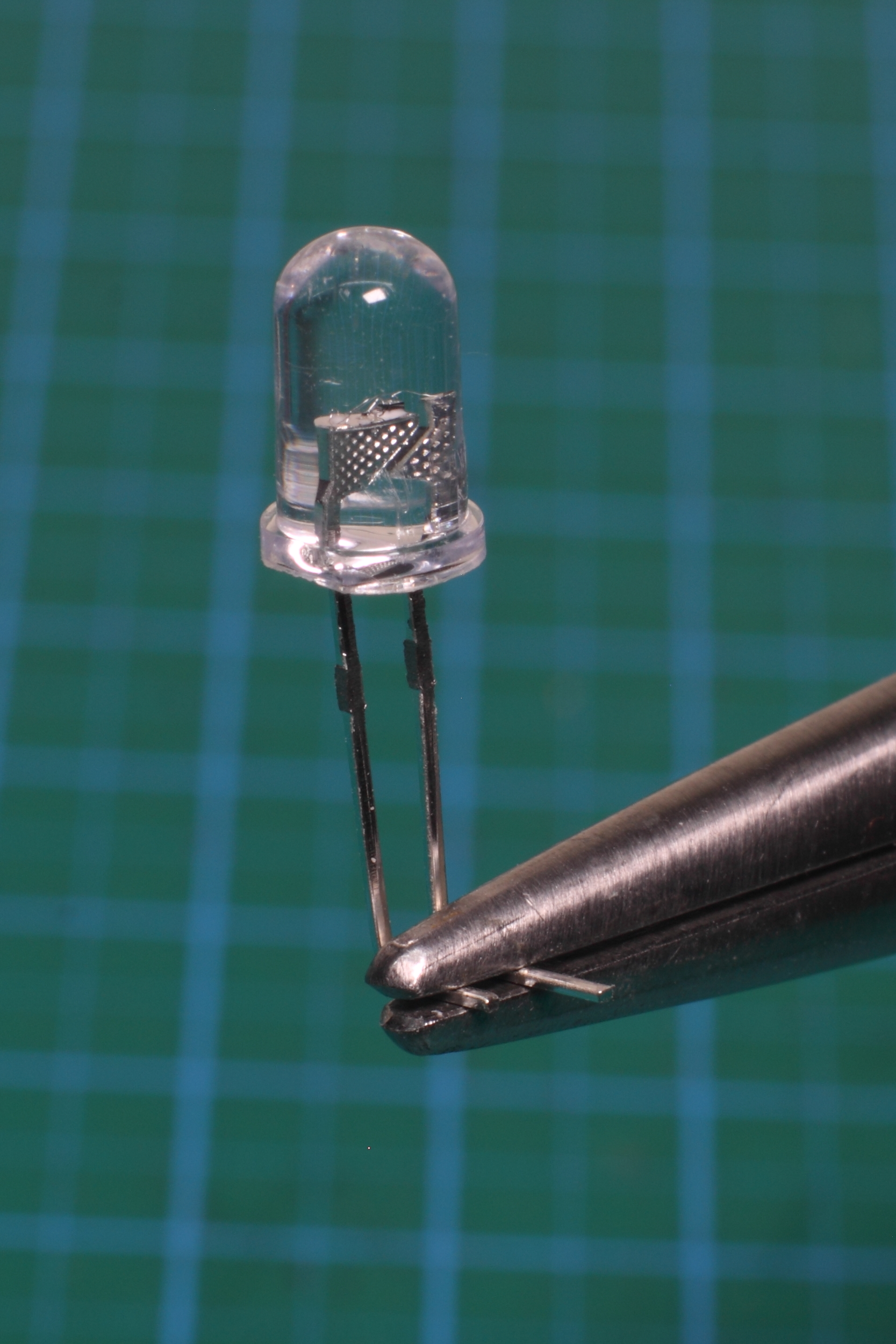
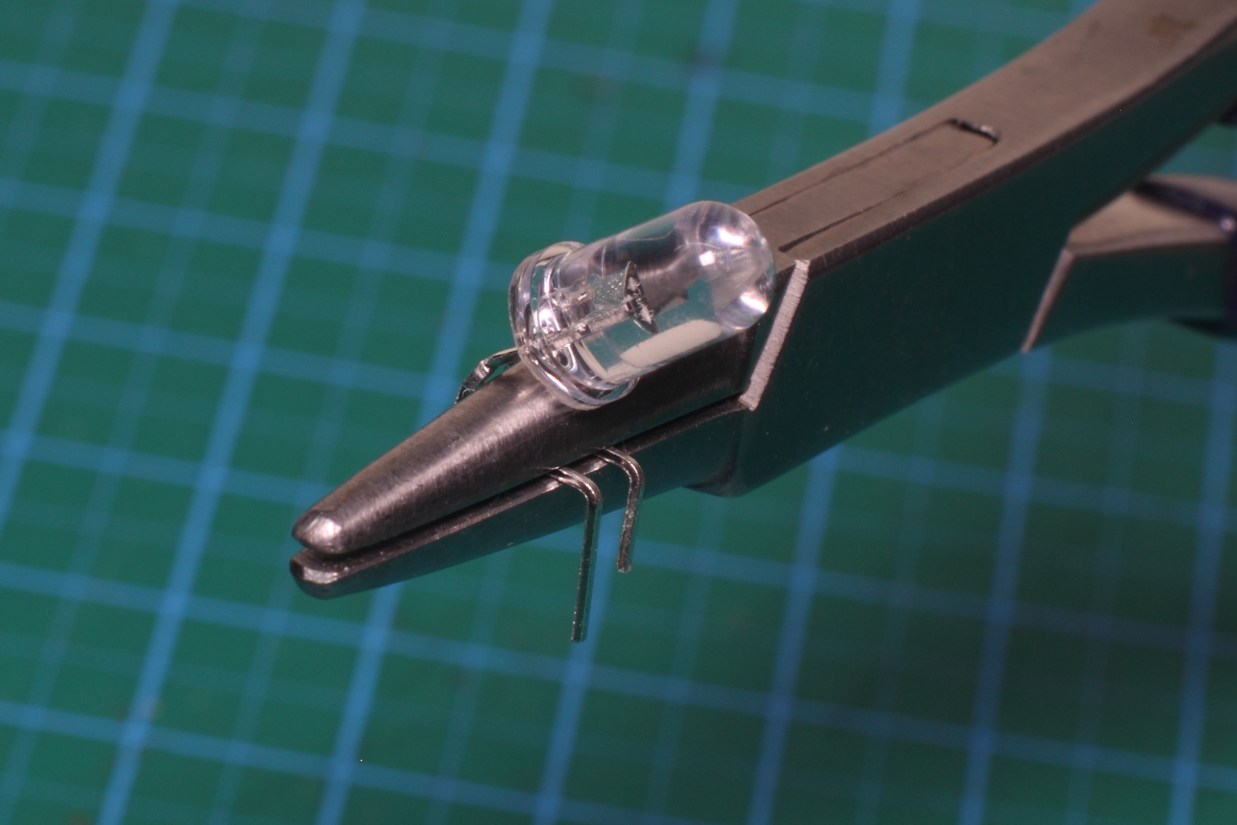
Bild 4–5: Vorverzinnen (Tinning)
Die nächsten beiden Bilder zeigen das Vorverzinnen:
-
der entsprechenden PCB-Pads
-
sowie der Kontaktflächen des Schalters und des Batteriehalters
Durch dieses Vorverzinnen lassen sich die Bauteile später leichter, schneller und sauberer verlöten – ein besonders hilfreicher Schritt für Anfänger*innen.
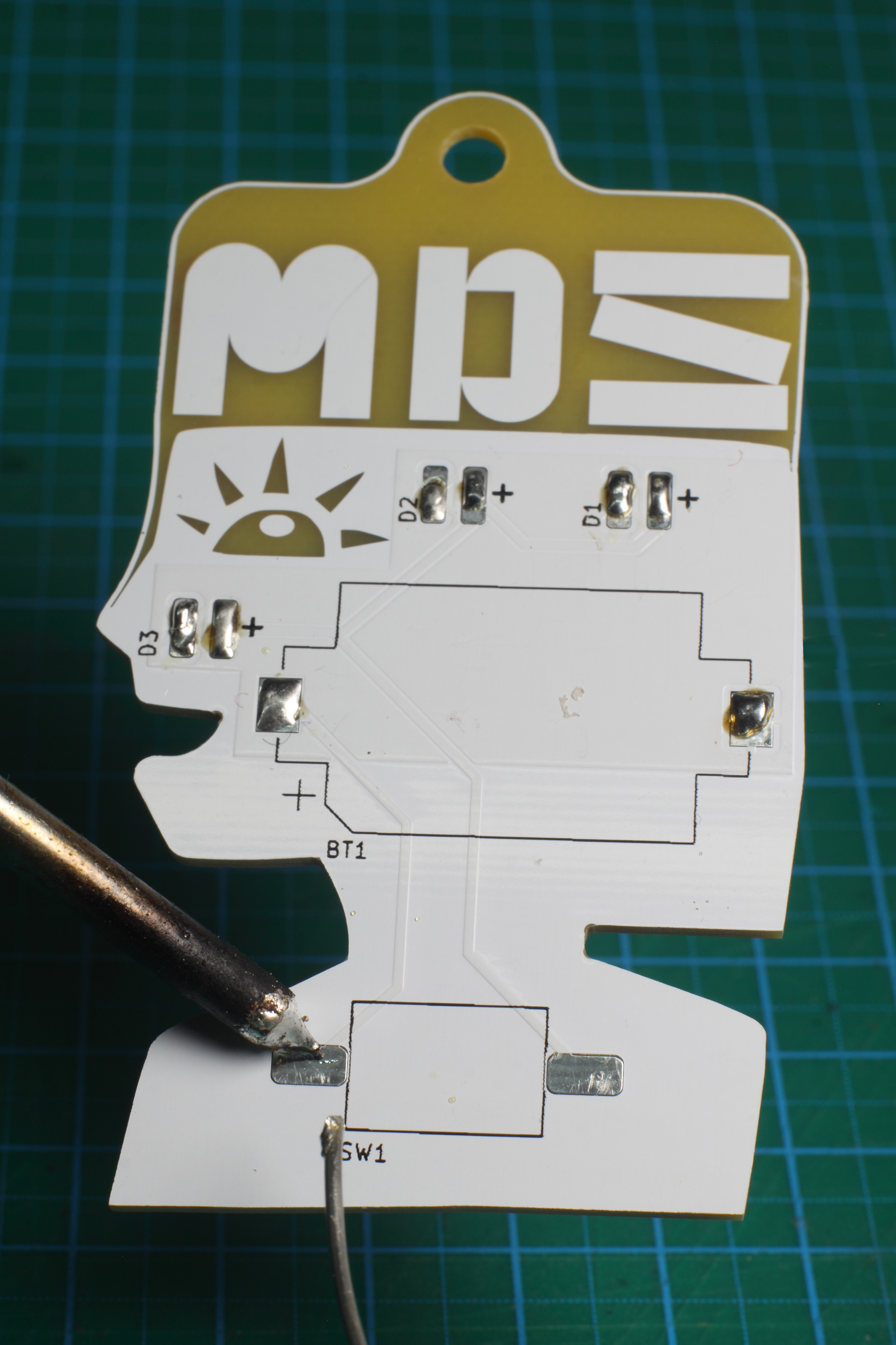
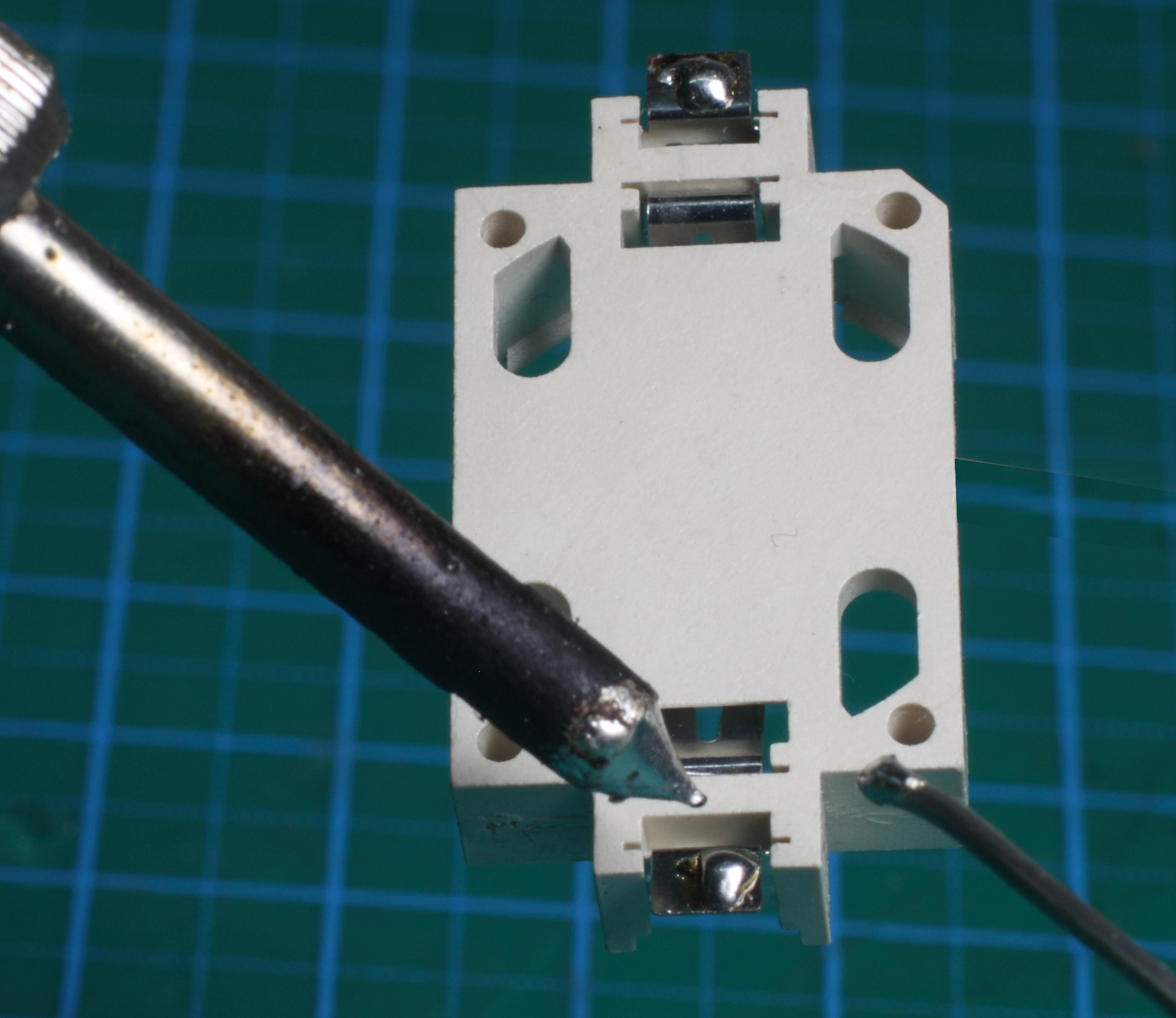
Bild 6: Fertig montiertes Badge
Das sechste Bild zeigt das vollständig aufgebaute und funktionsfähige Kit mit leuchtenden LEDs.
Dieses Bild dient als Referenz, wie das Endergebnis aussehen soll, und hilft bei der visuellen Kontrolle nach dem Zusammenbau.
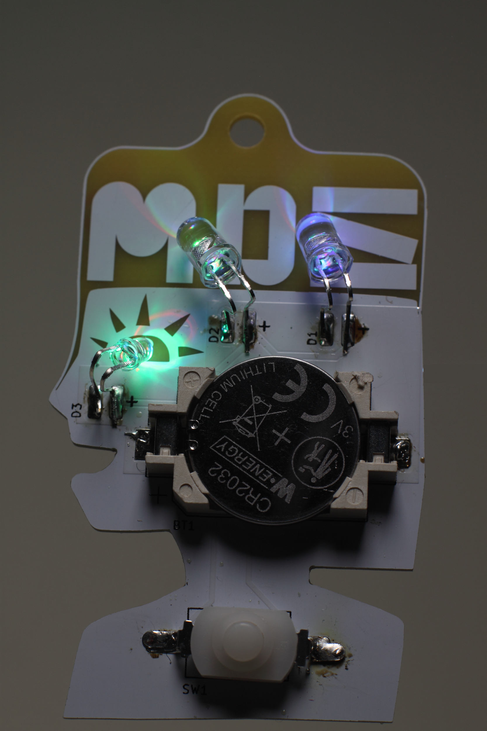
Bild 7: Optionaler Schritt – Lichtdiffusion mit Heißkleber
Das letzte Bild zeigt einen optionalen Zusatzschritt:
Die LEDs können mit transparentem Heißkleber ummantelt werden.
Dies hat den Effekt, dass:
-
das Licht über die Rückseite des PCBs weitergeleitet wird
-
ein weicherer, diffuser Leuchteffekt entsteht
Dieser Schritt ist rein optional und eignet sich besonders für Workshops, in denen zusätzlich mit Heißkleber gearbeitet wird oder ein stärkerer visueller Effekt gewünscht ist.