| **Time** | **Duration** | **Topic** |
| 10:00 | 30 | COVID Testing. Introduction, house rules. |
| 10:30 | 45 | Introduction to KiCad + Circuit Creation |
| 11:15 | 15 | break |
| 11:30 | 45 | Library Management - Symbols and Footprints |
| 12:15 | 60 | Lunch |
| 13:15 | 45 | Layout |
| 14:00 | 15 | break |
| 14:15 | 45 | Wrap up and packup |
| 15:00 | finish |
| **Time** | **Duration** | **Topic** |
| 10:00 | 30 | COVID Testing. Introduction, house rules. |
| 10:30 | 45 | Assembly |
| 11:15 | 10 | break |
| 11:25 | 45 | Assembly |
| 12:10 | 60 | Finish |
| [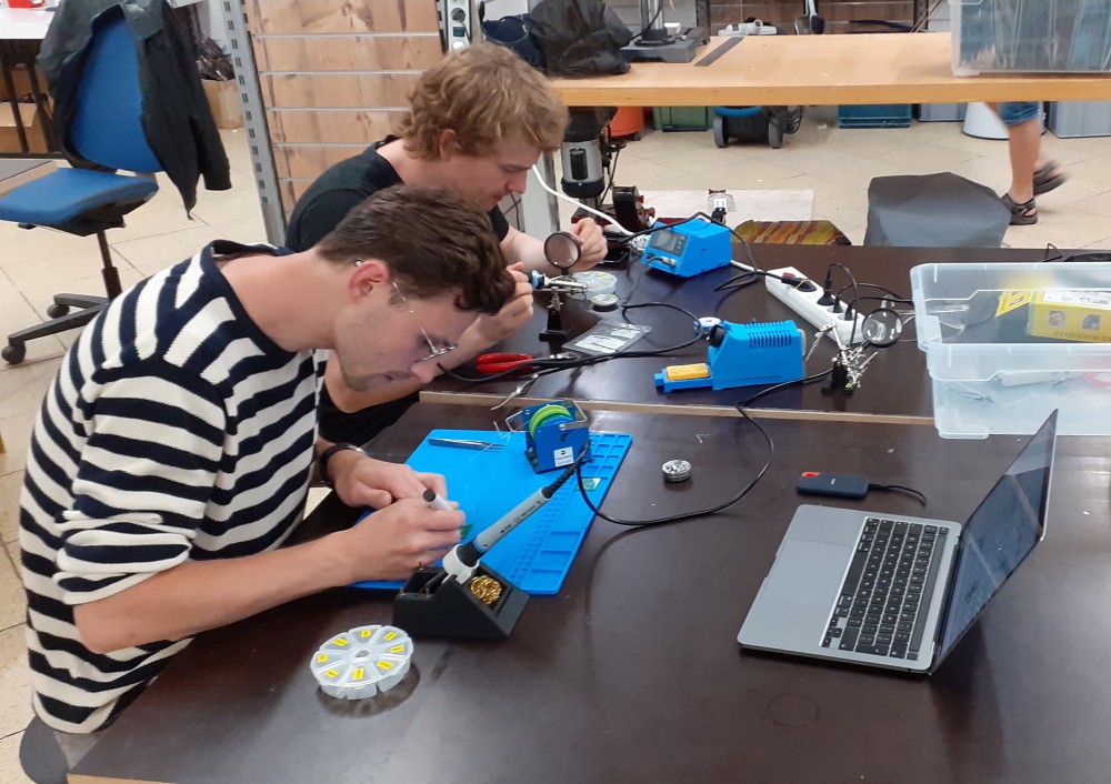](https://wiki.betreiberverein.de/uploads/images/gallery/2022-07/89ftt2A30WZQYLS0-img002.JPG) | 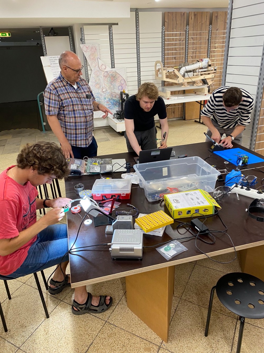 | [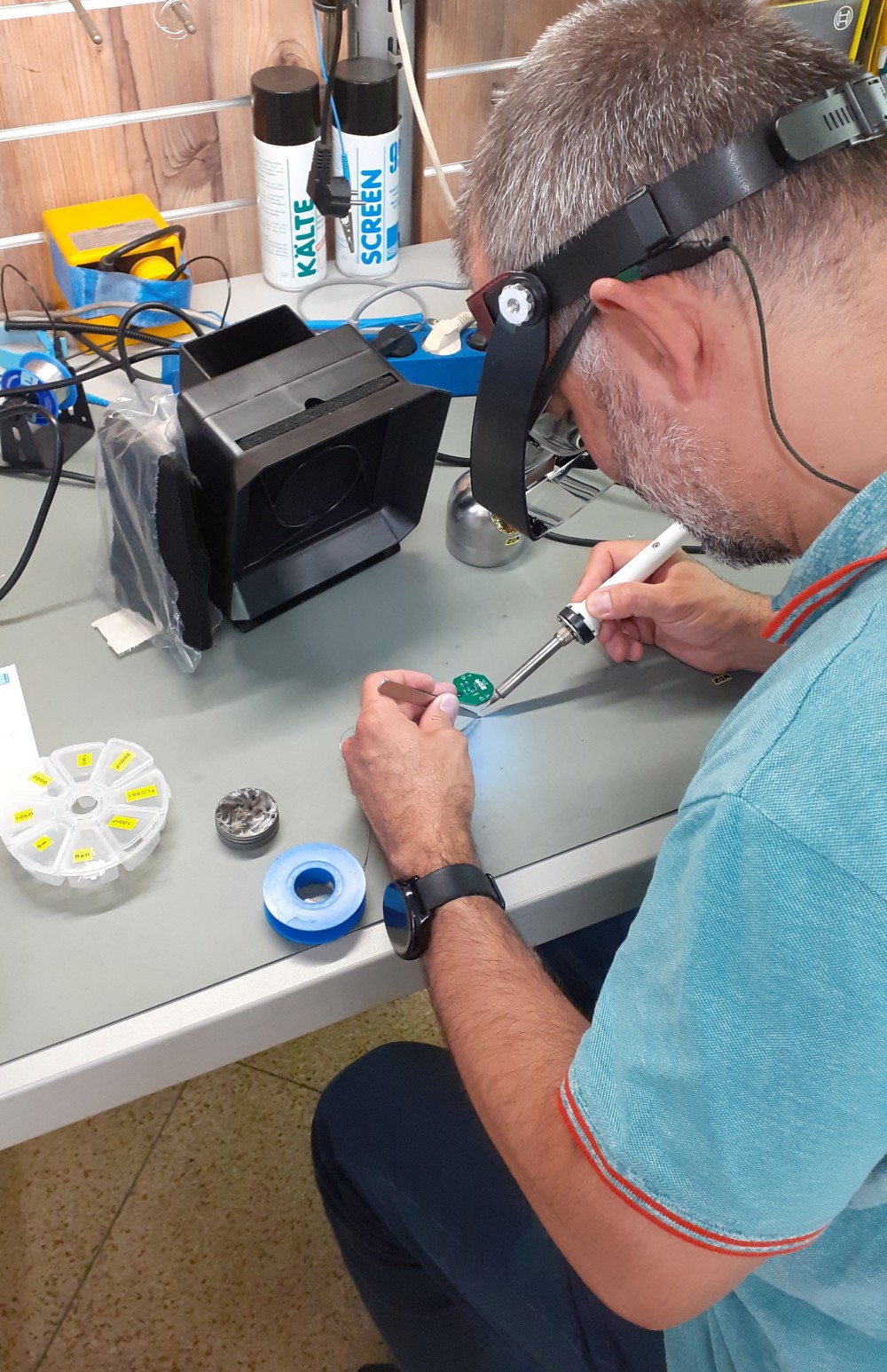](https://wiki.betreiberverein.de/uploads/images/gallery/2022-07/sZkmrhhnUbwr8HCc-img009.JPG) |
| [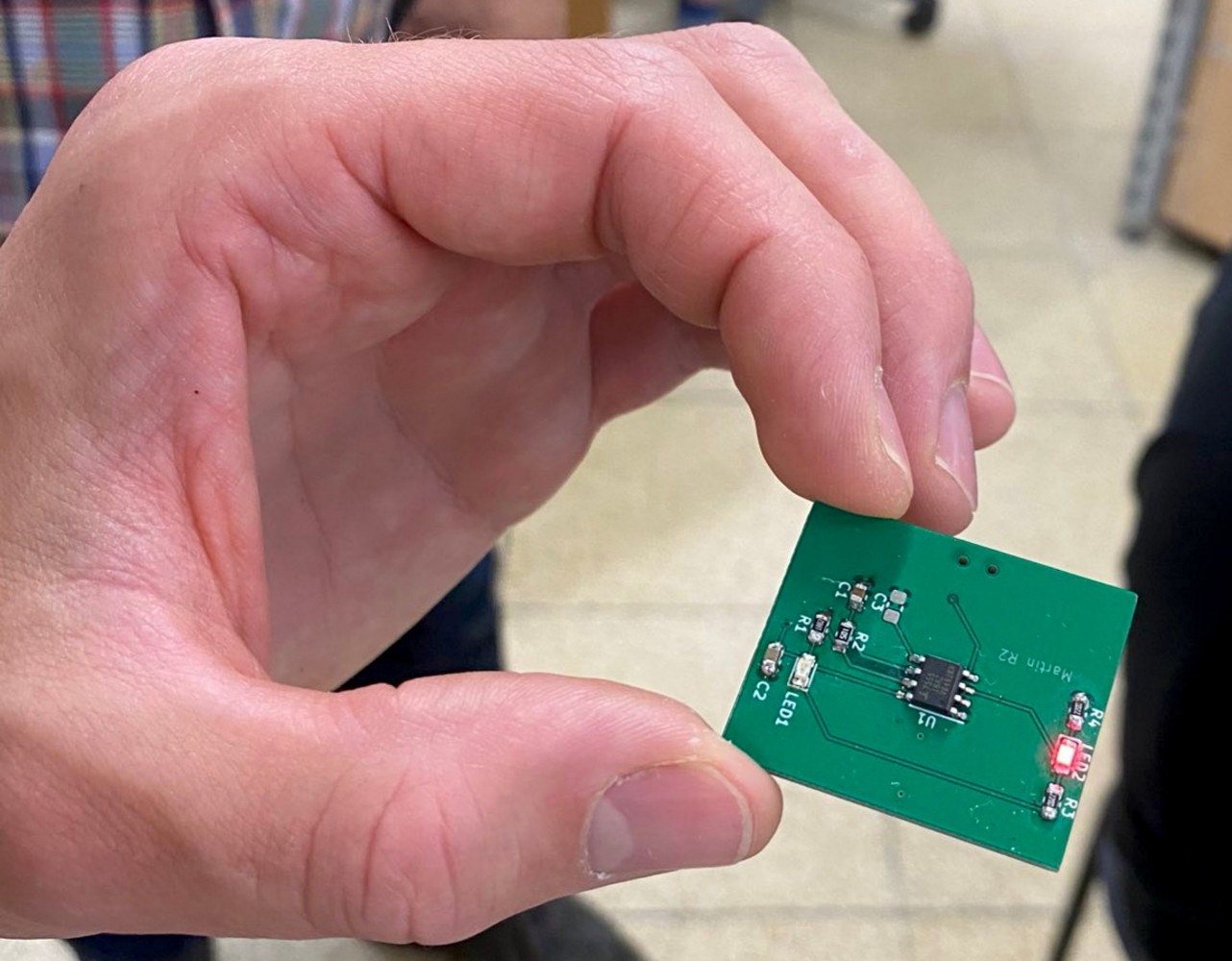](https://wiki.betreiberverein.de/uploads/images/gallery/2022-07/XRJyNKNsiYdCK14C-img004.JPG) | [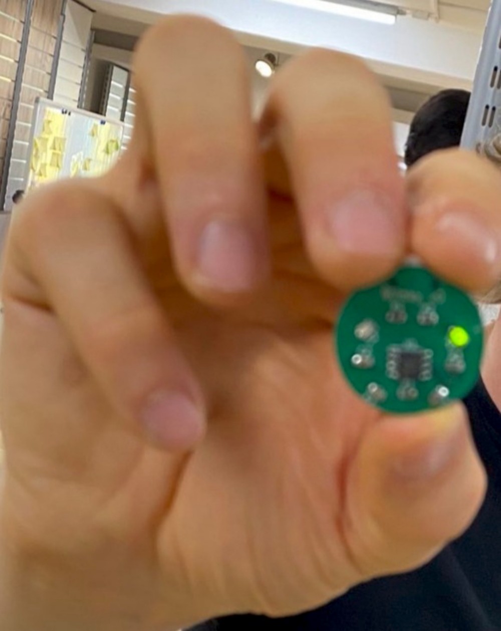](https://wiki.betreiberverein.de/uploads/images/gallery/2022-07/dS2OJ5vADXDQOceK-img005.JPG) | [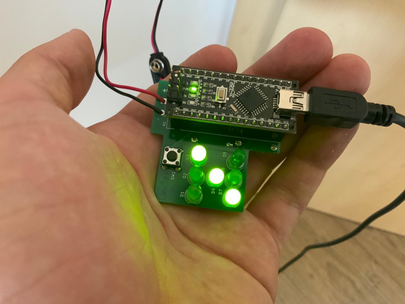](https://wiki.betreiberverein.de/uploads/images/gallery/2022-07/QmbEGZRUV5POyVa1-img006.JPG) |
| **Old** | **New** |
| [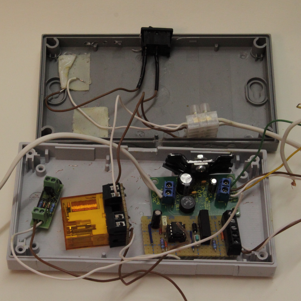](https://wiki.betreiberverein.de/uploads/images/gallery/2022-06/ZOmymBjxjtN35NgQ-theolddevice.png) | [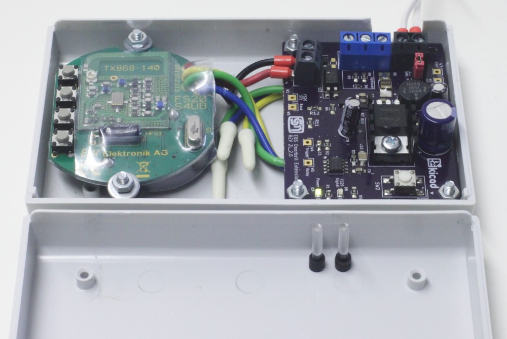](https://wiki.betreiberverein.de/uploads/images/gallery/2022-06/6bA51IHfz16CF7b1-img-0860e.JPG) |
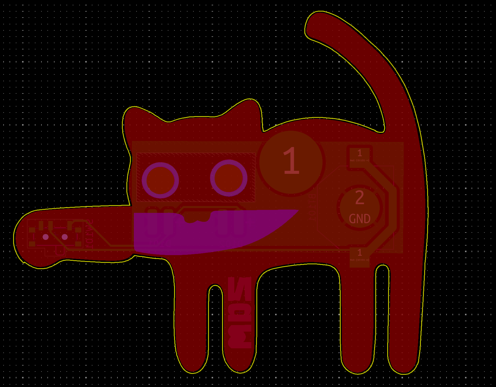
| [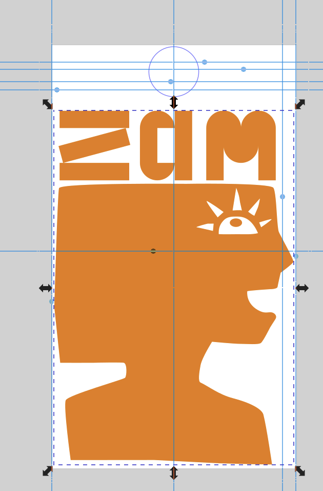](https://wiki.betreiberverein.de/uploads/images/gallery/2024-11/Vo8HhChCW1QWAI3a-front-cu.png) | The original image was exported as Front Copper (F.Cu). This will ensure that the section of the board that represents the *head* and letters will be opaque and not letter any light through. |
| [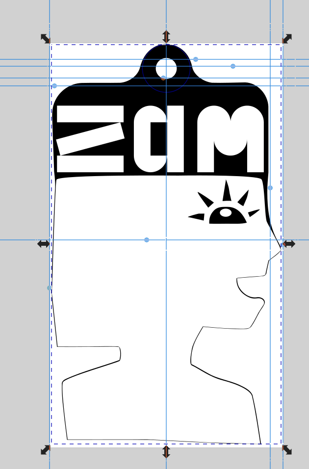](https://wiki.betreiberverein.de/uploads/images/gallery/2024-11/4BJcUp1XGB4wa2Lm-soldermask.png) | The next layer to export as the solder mask. For the entire image was exported but this has to be converted to a negative since this defines where the solder mask *should not go.* |
| [](https://wiki.betreiberverein.de/uploads/images/gallery/2024-11/S1YamFW2Yt1wxxyh-f-mask.png) | This image is then taken into a graphics program such as GIMP or Krita and trimmed down as the entire outline for this design. |
| [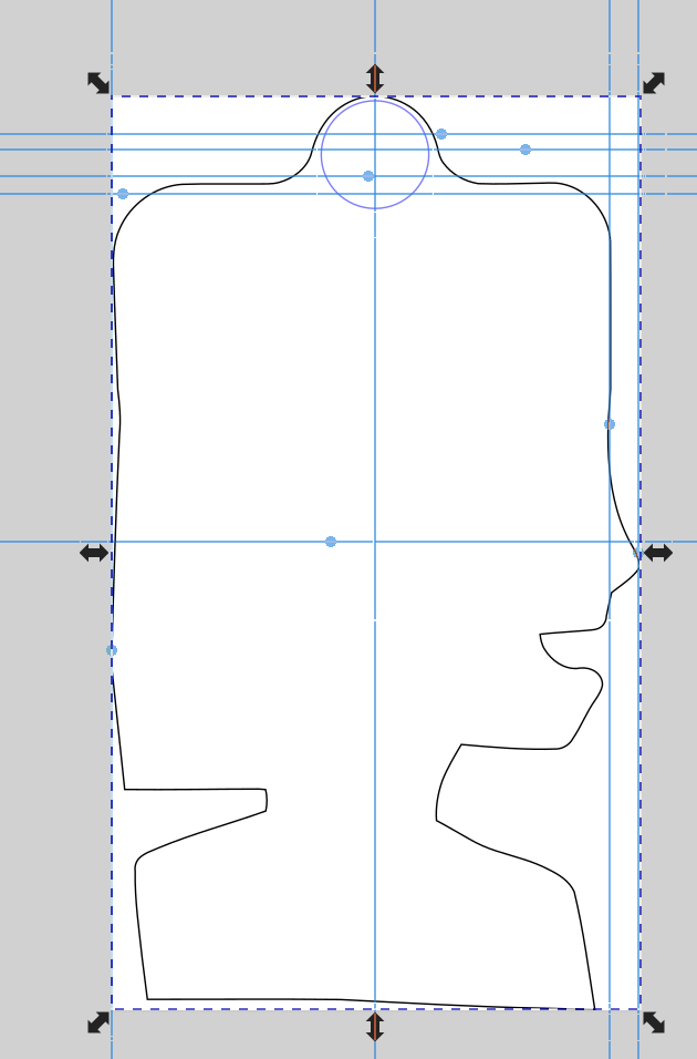](https://wiki.betreiberverein.de/uploads/images/gallery/2024-11/t1fODM2mXcWMy5rR-edgecut.png) | The last layer is based on the entire image and converted to an outline. This is then expanded using the *Outset* *tool*. This will ensure that milling tool following the edge cut will not conflict with the actual image outline. |
| [](https://wiki.betreiberverein.de/uploads/images/gallery/2025-02/PIO1xYuNkl85ILf4-image.png) | [](https://wiki.betreiberverein.de/uploads/images/gallery/2025-02/zOXM7cmAQt6wEGnD-image.png) |
| Edge Cut | Front Copper |
| [](https://wiki.betreiberverein.de/uploads/images/gallery/2025-02/AFmmodU5qdNZKx08-image.png) | [](https://wiki.betreiberverein.de/uploads/images/gallery/2025-02/PI2E2UzpBBRxAtDh-image.png) |
| Front Solder Mask | Back Solder Mask |
| [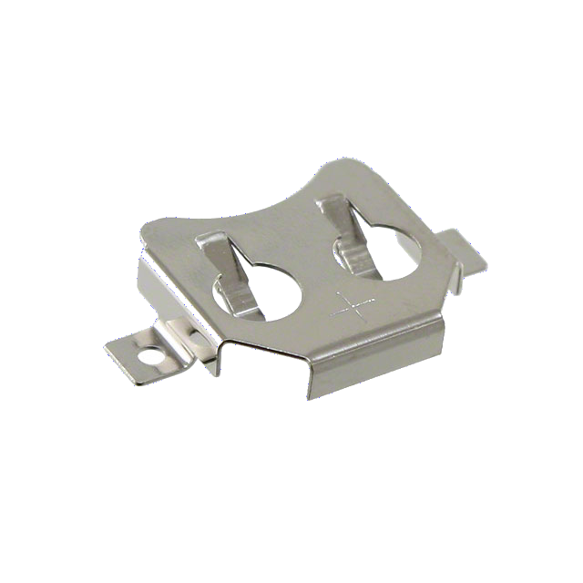](https://wiki.betreiberverein.de/uploads/images/gallery/2025-02/PYUeZBGg31KfjSwv-keystone-12mm.png) | [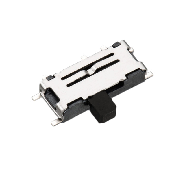](https://wiki.betreiberverein.de/uploads/images/gallery/2025-02/4udDhMUjed6lO54M-slide-switch.png) | [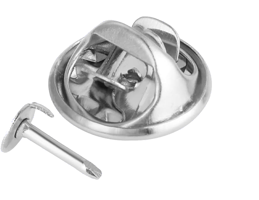](https://wiki.betreiberverein.de/uploads/images/gallery/2025-02/n58tcUZ8tVQ6FiRr-butterfly-pin.png) |
| [](https://wiki.betreiberverein.de/uploads/images/gallery/2025-02/v0KjVosPUH9DUV4L-image.png) | [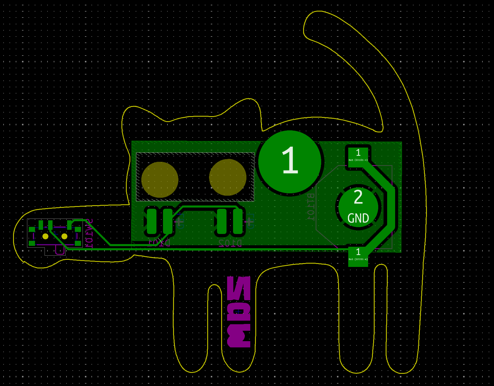](https://wiki.betreiberverein.de/uploads/images/gallery/2025-02/nIak3ofN0MOCZz85-image.png) |
| PCB design with front copper pour | PCB design without the front copper pour, showing the back copper. |
| [](https://wiki.betreiberverein.de/uploads/images/gallery/2025-02/SoIADt83VPv8L4tl-image.png) | [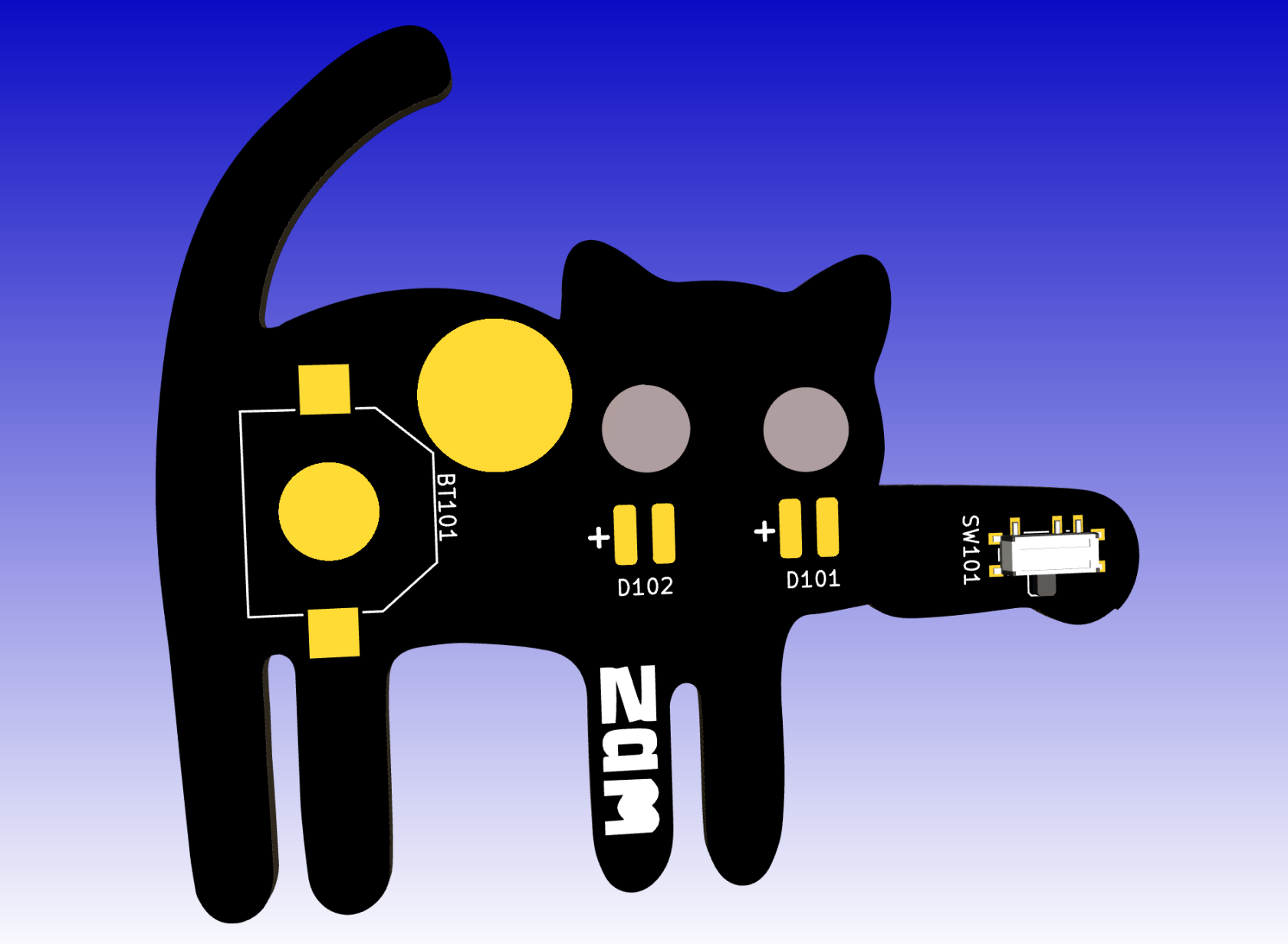](https://wiki.betreiberverein.de/uploads/images/gallery/2025-02/fHXyGp8f5s9lrA2K-image.png) |
| 3D view of the final design | 3d view of the back side of the PCB |
| [](https://wiki.betreiberverein.de/uploads/images/gallery/2025-03/rpnuNpyvSVxn8ieI-img-2660.JPEG) | [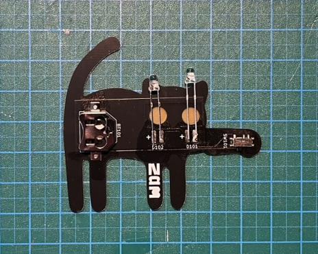](https://wiki.betreiberverein.de/uploads/images/gallery/2025-03/z1zho7A5gdD1wLC6-img-2661.JPEG) |
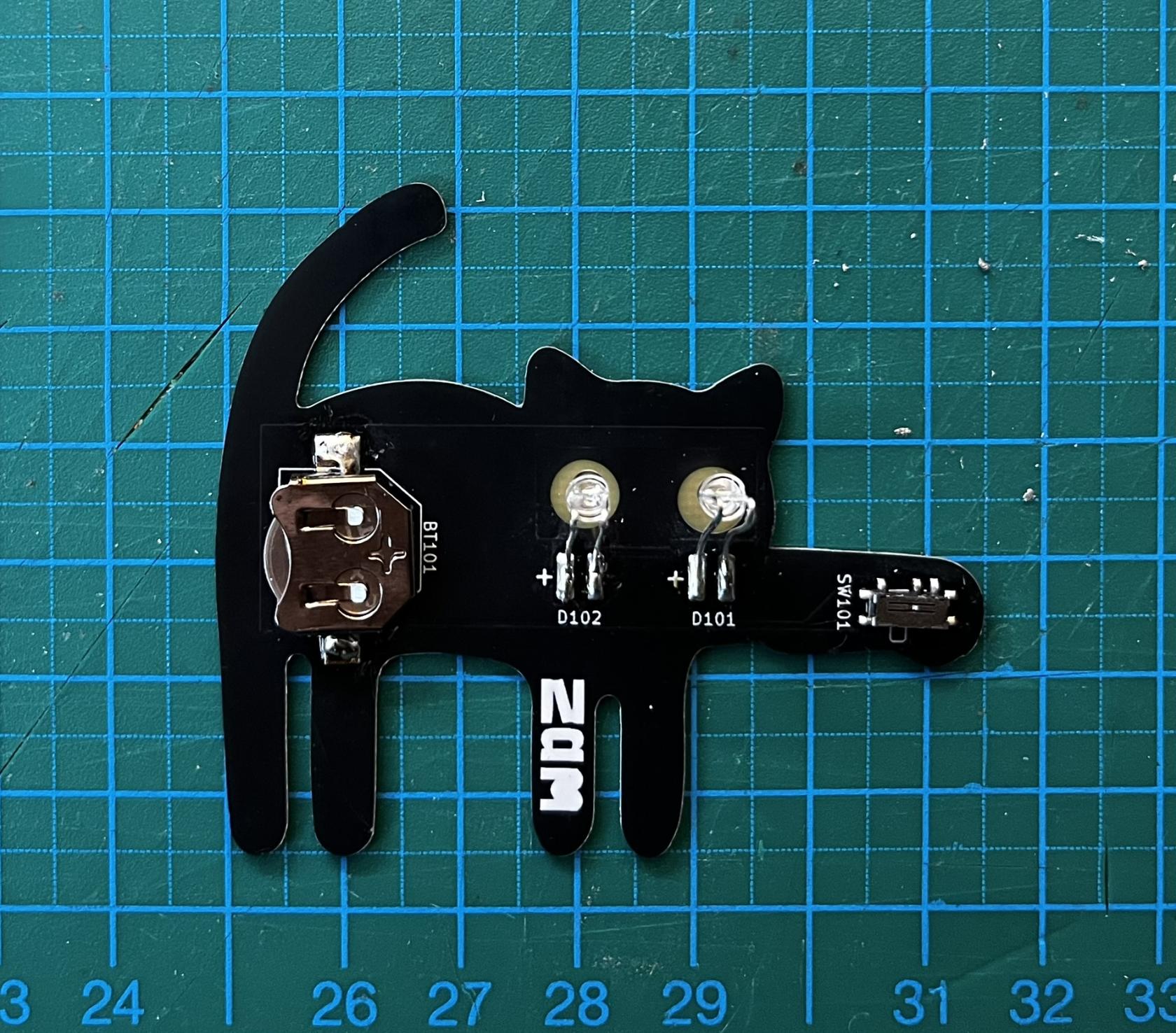
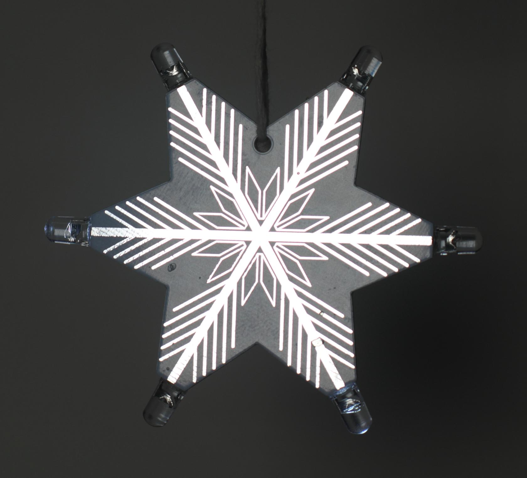
| For this build, 3mm slow blinking LEDs were chosen. Equally, any though-hold LED can be used. |
| [](https://wiki.betreiberverein.de/uploads/images/gallery/2025-03/NJ8CZMw5juEKoUAl-img-2668.JPEG) | [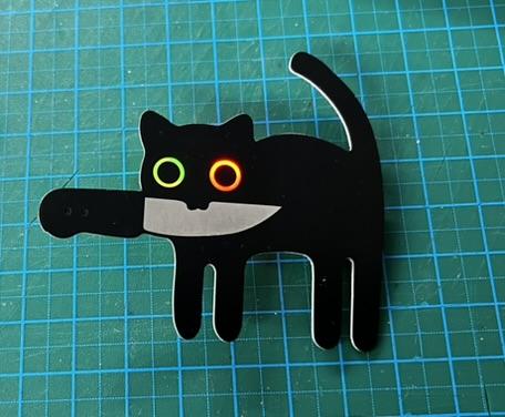](https://wiki.betreiberverein.de/uploads/images/gallery/2025-03/ozgB5B0Ego6nEv0m-img-2666.JPEG) |
| The assembled parts with the LEDs bent into position |
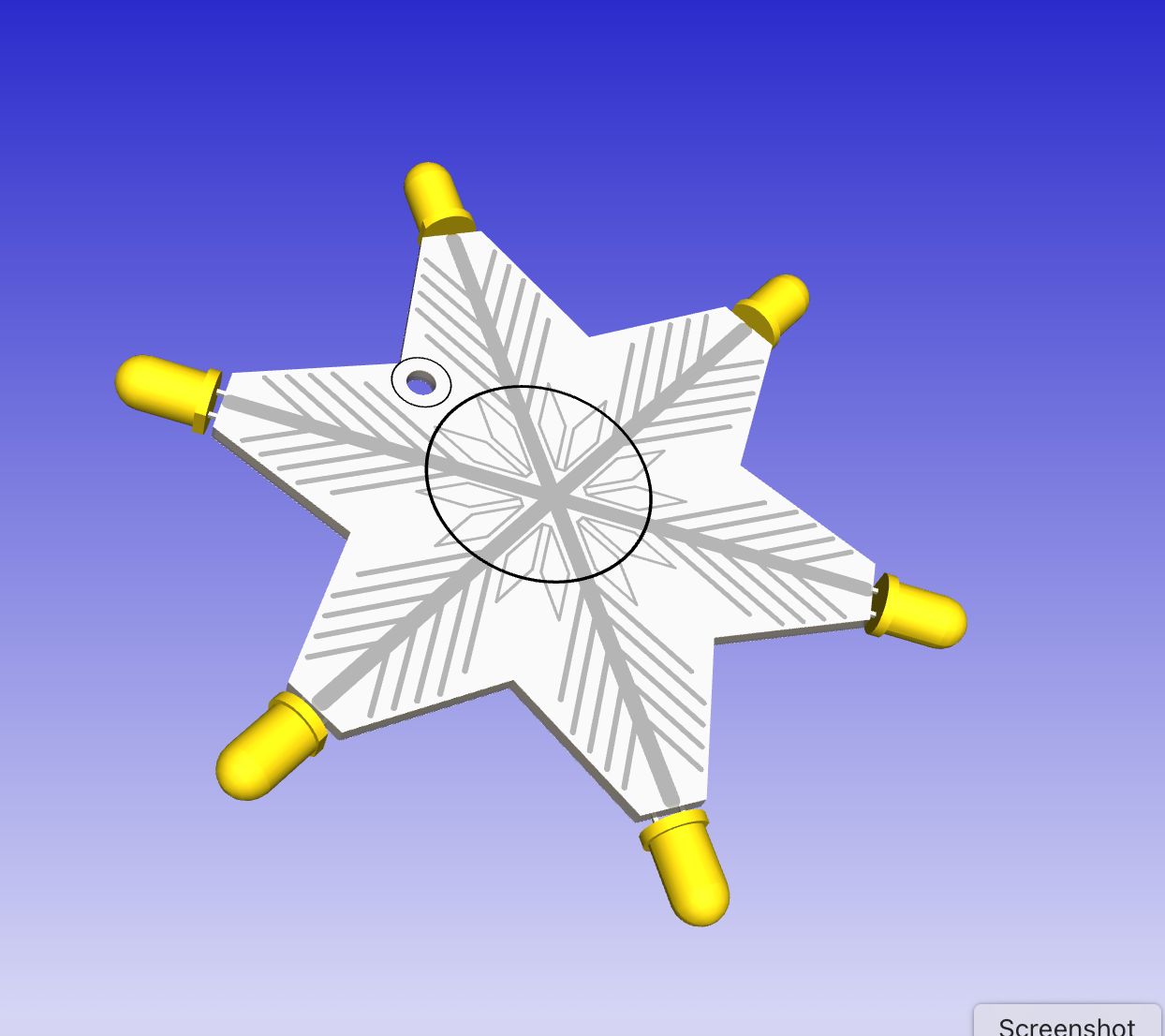
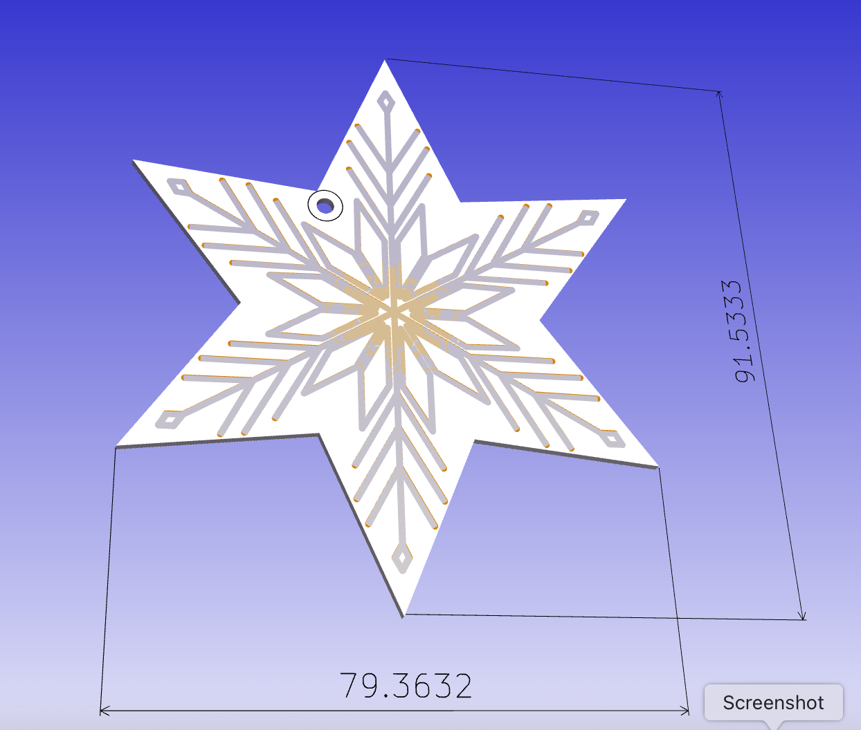
| **Motivation / Grundidee** | Im Rahmen einer öffentlichen Vorweihnachtsveranstaltung im offenen Werkraum ZAM wurden Familien und insbesondere Kinder eingeladen, gemeinsam kreative Aktivitäten rund um die Advents- und Weihnachtszeit durchzuführen. Ein Schwerpunkt lag dabei auf dem Basteln und Gestalten von Sternen als adventliche Dekoration. Vor diesem Hintergrund entstand der Wunsch nach einer einfachen, kindgerechten Einführung in das Löten. Ziel war es, Leiterplatten (PCBs) zu entwerfen, die thematisch zum Advent passen, robust genug für Anfänger:innen sind und gleichzeitig einen sichtbaren, motivierenden Erfolg bieten. Analog zum bereits bekannten [ZAM Badge 2024](https://wiki.betreiberverein.de/books/projekte-aktuell/page/zam-badge-2024) sollten die Platinen als eigenständige Lötübungen dienen. Das Ergebnis sind zwei Stern-PCB-Designs (fünf- und sechszackig), die mit blinkenden LEDs bestückt werden und nach dem Löten als leuchtende Adventssterne genutzt werden können. |
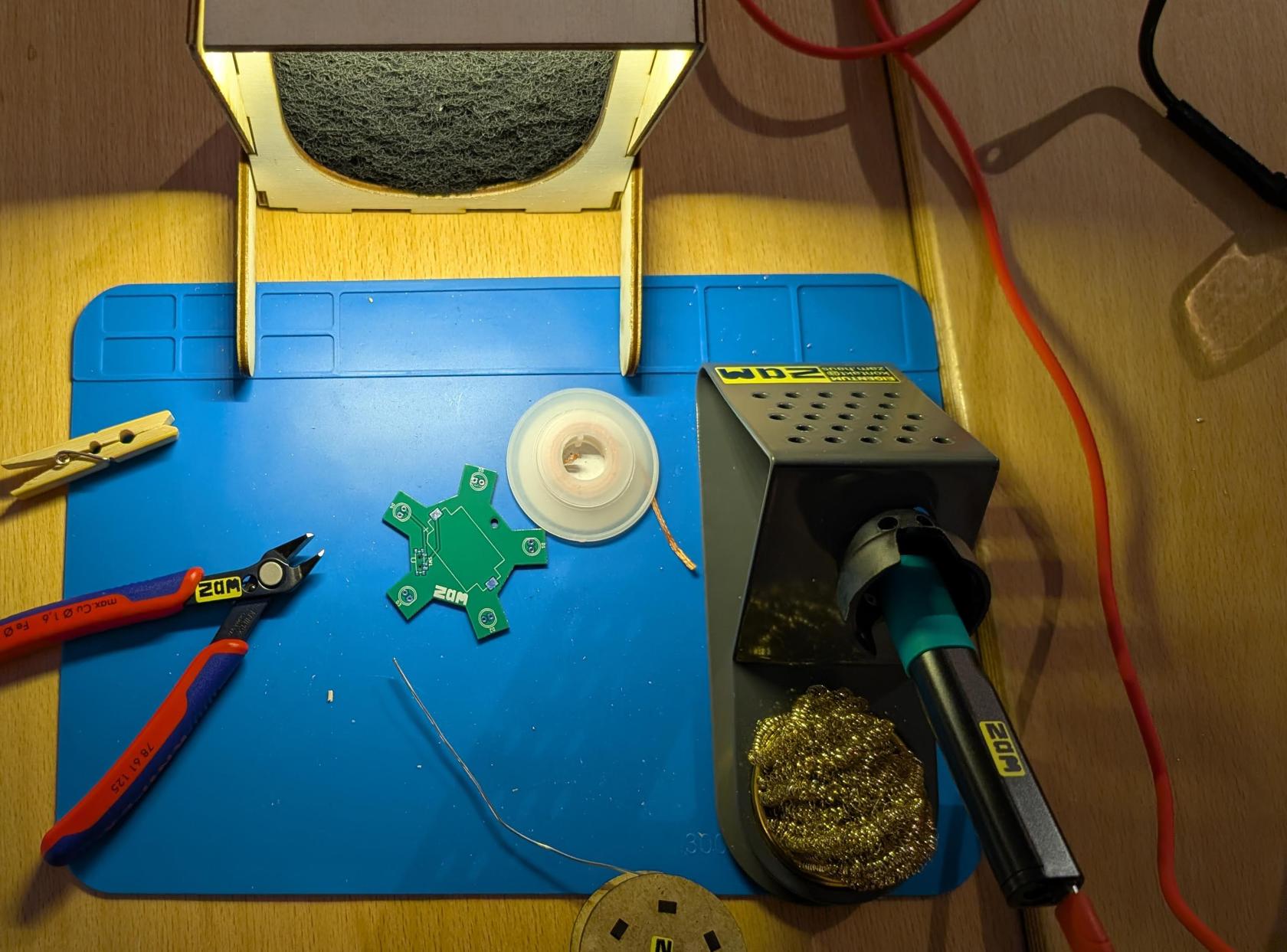
| **Platzbedarf** | Für die Durchführung der Advent-Löt-Aktion wird kein dauerhafter Platz benötigt. Die Aktivität kann an vorhandenen Werkbänken im ZAM durchgeführt werden. Benötigt werden pro Arbeitsplatz: - ca. 1 m² Tischfläche - Lötstation (Lötkolben, Halter, Schwamm) - Lötzinn - Seitenschneider - Dunstabzug |
| **Ab wann / wie lange** | - Projektstart (Designphase): November 2025 - PCB-Design & Fertigung: ca. 1–2 Wochen - Lötaktion / Event: Dezember 2025 (Vorweihnachtszeit) Die eigentliche Lötübung pro Stern dauert – je nach Erfahrung – etwa 15–30 Minuten. |
| **Kontakt** | Name: Steve Mayze @smayze Projekt: ZAM Advent Star GitHub: https://github.com/SteveMayze/ZAM-Advent-Star |
| [](https://wiki.betreiberverein.de/uploads/images/gallery/2025-12/LeLFWYEeJ8JjQeXp-screenshot-2025-11-25-at-10-11-48-95hjfe67xfdr8yobnyi77w68we.png) | [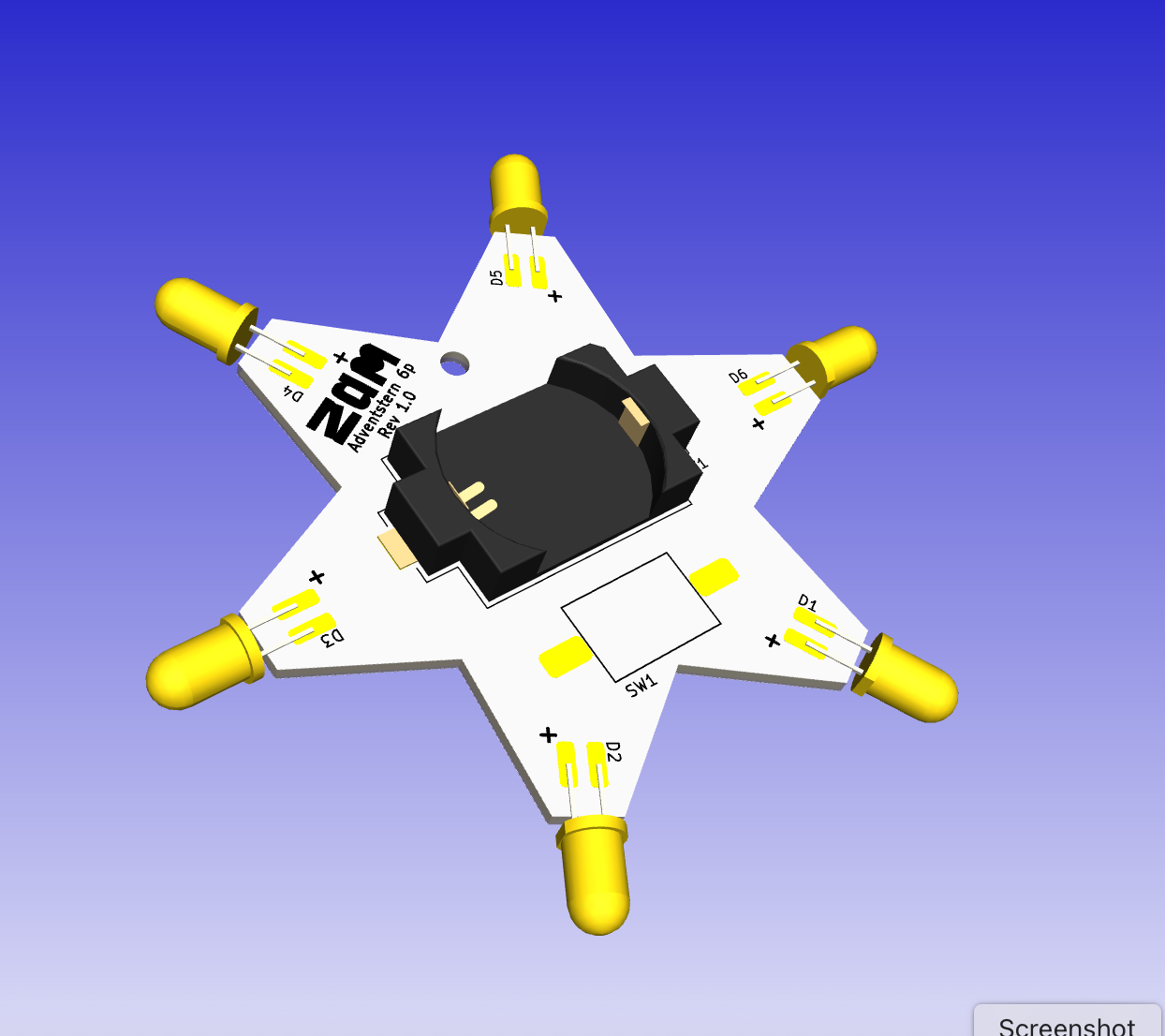](https://wiki.betreiberverein.de/uploads/images/gallery/2025-12/BupDQZ6PD3W16sFn-screenshot-2025-11-25-at-10-12-10-kjnnst457fgdmdaqhm6myknm9o.png) |
| [](https://wiki.betreiberverein.de/uploads/images/gallery/2025-12/1o5Lwkcp31yII5S2-screenshot-2025-11-23-at-17-15-41-8p9ewqgadfnauyh5ftzk6xiidy.png) | [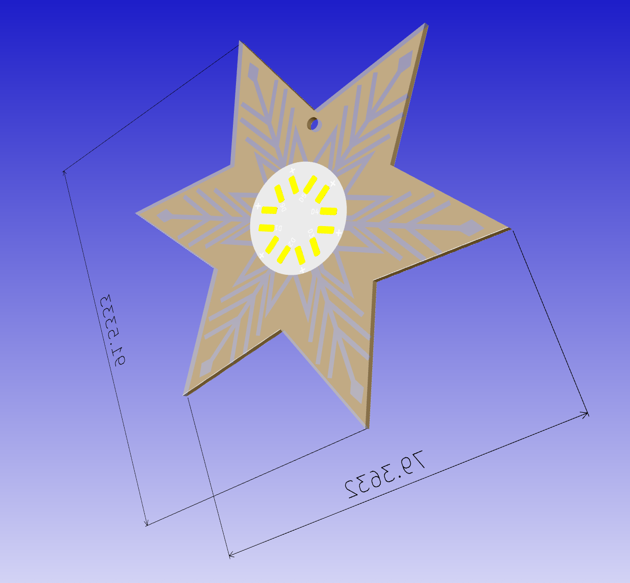](https://wiki.betreiberverein.de/uploads/images/gallery/2025-12/tJ2jARItlqEj38BH-screenshot-2025-11-23-at-17-15-57-41hp4arrep89je36mdxowq4ogr.png) |
| [](https://wiki.betreiberverein.de/uploads/images/gallery/2025-12/LeLFWYEeJ8JjQeXp-screenshot-2025-11-25-at-10-11-48-95hjfe67xfdr8yobnyi77w68we.png) | [](https://wiki.betreiberverein.de/uploads/images/gallery/2025-12/BupDQZ6PD3W16sFn-screenshot-2025-11-25-at-10-12-10-kjnnst457fgdmdaqhm6myknm9o.png) |
| [](https://wiki.betreiberverein.de/uploads/images/gallery/2026-01/C0hnKmUmBiknOWqG-pxl-20251213-151836908.jpg) | |
| [](https://wiki.betreiberverein.de/uploads/images/gallery/2026-01/lfqjgHDpgeaZ4Uf7-img-0065.JPG) | [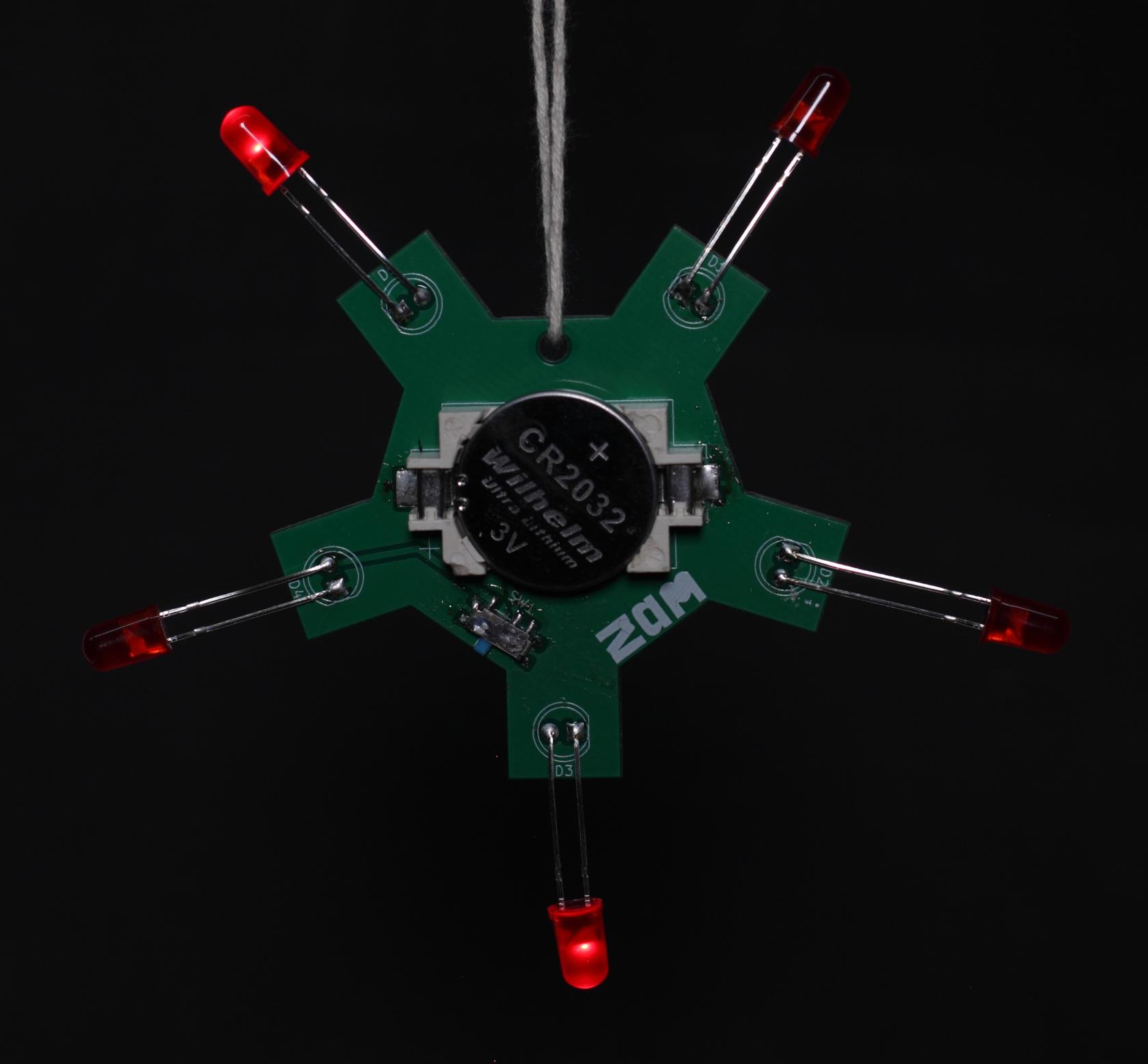](https://wiki.betreiberverein.de/uploads/images/gallery/2026-01/Wuqix3C3LuplbzyU-img-0073.JPG) |
| **Motivation / Grundidee** | Das **ZAM Badge Soldering Kit** ist ein einfaches Löt-Kit, das bei ZAM-Events, Workshops und offenen Tagen eingesetzt werden kann. Ziel ist es, **einen niedrigschwelligen Einstieg ins Löten und in Elektronik** zu ermöglichen – auch für Anfänger\*innen und Kinder (ab ca. 7 Jahren mit Unterstützung). Auslöser für das Projekt war der Wunsch nach: - einem **einheitlichen, wiederverwendbaren Bastel-/Workshop-Projekt** - einem **sichtbaren ZAM-Artefakt** (Badge), das Besucher\*innen mitnehmen können - einem **didaktisch sinnvollen Einstiegsprojekt**, das schnell Erfolgserlebnisse bietet Das Kit basiert auf dem bestehenden [**ZAM Badge 2024 PCB**](https://wiki.betreiberverein.de/books/projekte-aktuell/page/zam-badge-2024) [](https://wiki.betreiberverein.de/books/projekte-aktuell/page/zam-badge-2024) Für das Soldering Kit wird dieses Design so aufbereitet, dass: - alle Bauteile **bedrahtet** und gut lötbar sind - die Stückliste überschaubar bleibt - das Ergebnis direkt funktioniert (z. B. LED(s), einfacher Effekt) Bestandteile des Kits: - ZAM Badge PCB - alle benötigten elektronischen Bauteile - optional: Sticker - kurzes Info- und Montageblatt (1 Seite, bebildert) |
| **Platzbedarf** | Für die **Herstellung der Kits**: - kein dauerhafter Platzbedarf - temporärer Arbeitsplatz (z. B. Werkbank oder Tisch) zum: - Sortieren der Bauteile - Zusammenstellen der Kits - Verpacken (Beutel) Für den **Einsatz bei Events / Workshops**: - Tischfläche pro Person ca. **40 × 60 cm** - Lötstation(en), Stromanschluss - typische Workshop-Umgebung im ZAM ausreichend |
| **Ab wann / wie lange** | **Projektstart:** bereits erfolgt (basierend auf ZAM Badge 2024) Geplanter Ablauf: - Vorbereitung / Anpassung PCB & Stückliste: abgeschlossen - Bestellung der Bauteile: erfolgt - Zusammenstellung der Kits: ca. **1–2 Stunden pro 200** - Erstellung der Kurzanleitung: ca. **2–3 Stunden** Das Projekt ist **laufend nutzbar** und kann bei Bedarf immer wieder neu aufgelegt werden. |
| **Kontakt** | Name: *Steve Mayze* Telefon / Mattermost: @smayze Name: *Jochen Hunger* Telefon / Mattermost: @jochen.hunger Name: *Britta Wachler* Telefon / Mattermost: @britta.wachler |