KiCad Basics Teil 1. Samstag 04.06.22
Teil 1. Platine Herstellen
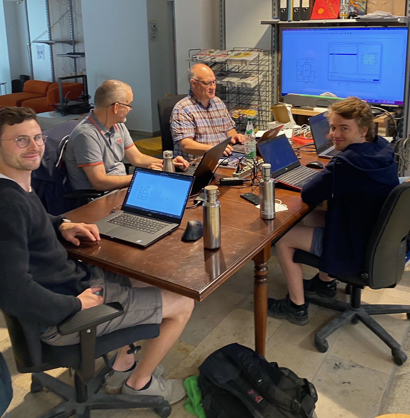
On Saturday 04.06.22 Steve held his first KiCad workshop in ZAM.
There were two goals for the event.
- Introduce the attendees the work-steps required to create a PCB. This workflow is not unique to KiCad.
- Have a set of design files ready to send for fabrication.
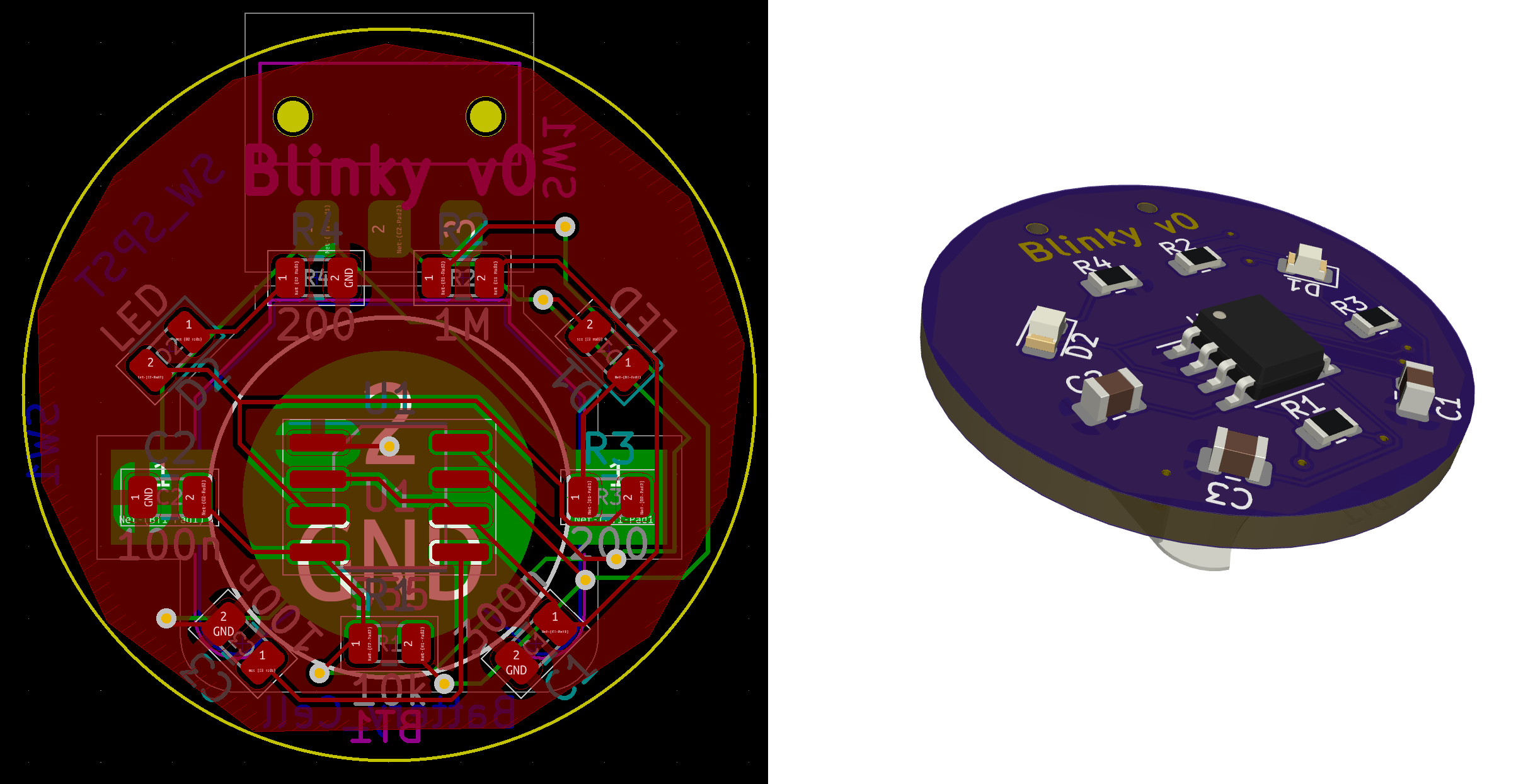
A relatively simple (but not too simple - Falstad model) project was presented. The classic first project, a blinking LED project. 
There was quite a bit of information to get through.
- Creating a project.
- Creating a schematic.
- Creating and modifying the symbols for a schematic.
- Assigning footprints to the symbols.
- Creating and modifying the footprints.
- Creating the layout.
Steve will be sending what design files are available off for fabrication the coming Wednesday so that they will be ready for Part 2. The Assembly and Testing of the boards.