KiCad Basics Teil 1. Samstag 04.06.22
Teil 1. Platine Herstellen
Steve Mayze
Objective
The creation of projects in electronics requires the connection of various components to build a circuit. There are various means to achieve this - breadboard, verro-board. However there are many advantages to building an own Printed Circuit Board (PCB). The purpose of this workshop was to introduce the attendees to the KiCad electronic design tool so that they will gain the know-how and confidence to create their own PCBs.
There were two goals for the event.
- Introduce the attendees the work-steps required to create a PCB. This workflow is not unique to KiCad.
- Have a set of design files ready to send for fabrication.
Method
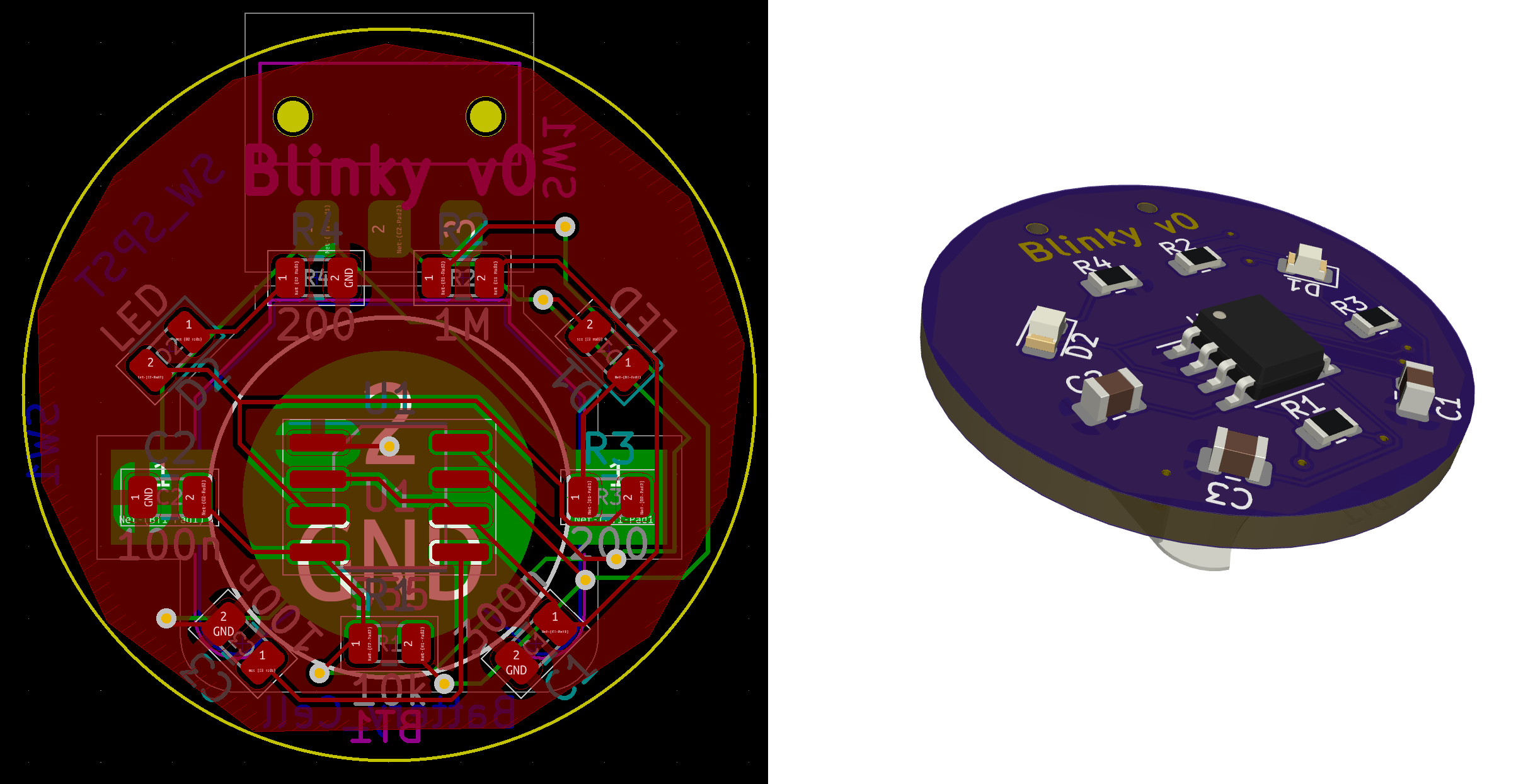
A relatively simple (but not too simple - Falstad model) project was presented. The classic first project, a blinking LED project. The project was presented as our final goal that we needed to implement as a PCB.

There was quite a bit of information to get through.
- Creating a project.
- Creating a schematic.
- Creating and modifying the symbols for a schematic.
- Assigning footprints to the symbols.
- Creating and modifying the footprints.
- Creating the layout.
Procedure
I opened the session with the question of why do we ant to create our own PCB? The answers that came back were consistent to what drew me into this area of electronic development.
- DIY home automation.
- Neatening up existing projects.
- Wanting to interface neatly with existing development boards.
- Create my own development board.
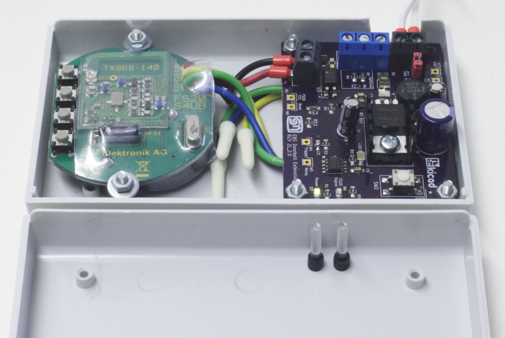
I showed my won example of neatening up a project. Where I presented a first attempt at creating my won door bell extension with what I knew at the time and using Verro board.
| Old | New |
 |
 |
We then started work. I introduced the software and the creation of the schematic diagram with an introduction to the symbol library and how you go about creating a new symbol or changing an existing one to suite the purpose of the diagram. It soon came apparent that a symbol does not need to exactly match the physical component that is going to be used in the circuit. The schematic is a design document to help the developer and other understand the operation of a circuit.
After lunch we moved onto the PCB Layout itself. Ideally the purpose of the class. I showed how to prepare the schematic for import into the PCB layout tool and to make a start on the layout and a couple of things to watch out for like understanding the design limitations and tolerances of the PCB fabrication house. This means before we start, to set up the minimum distances and widths allowed for the copper.
There is the question if this was a PCB creation workshop, how come we are preparing the design files to send off for fabrication? The answer is that the actual fabrication of the physical PCB is only one part of the process and actually not a significant part of the overall creative process of creating the design, assembling and troubleshooting. There is more than one technique for creating a PCB and ZAM does not yet have the facilities for either of these processes. Sending the boards off for fabrication is the simplest and most effective way to introduce the more important aspects of the creative process.
So at the end of the session, we now have some design files that can be sent off and on their return we will continue with the second part - the assembly and testing of the boards.