ZAM Badge 2024
Überblick
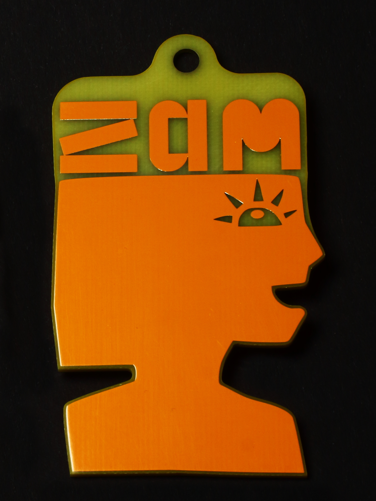
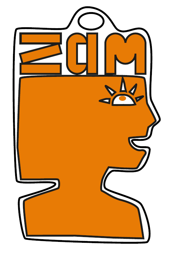
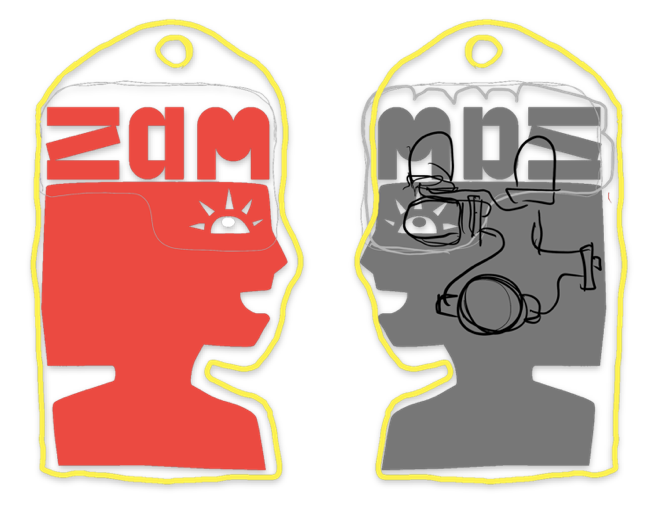
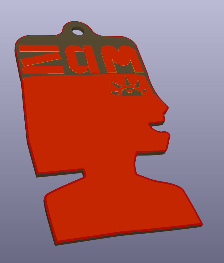
Bei der Planung des VULCA-Treffens kam die Idee eines Badge als Konferenzpräsent und Lötübung auf. Die Idee besteht darin, die folgende Grafik zu nehmen und diese in eine Leiterplatte mit blinkenden LEDs hinter dem Auge und den Buchstaben umzuwandeln.

Projekt-Metadaten
ZAM-Badge-24 GitHub Repository
Jochen Hunger jochen.hunger@betreiberverein.de
Steve Mayze smayze@yahoo.com
Logbuch / Schritte
Tag 1 Zusammenarbeit
Erstens
warI dieturned Vorstellungen.graphics
PCBs before but I was further inspired by Working with artists to design beautiful boards at KiCon Europe 2024. The first thing was to come up with the concept. Given the original graphic, I outlined a possible arrangement of the PCB layers.
DannBased kamn dasthis, Koncept
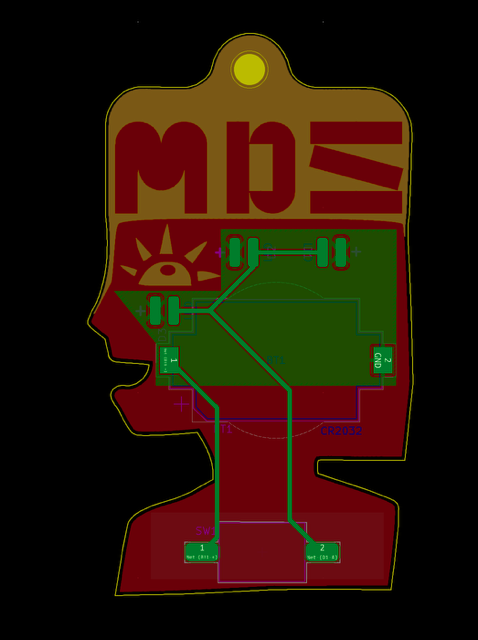
proposed what he was thinking. This would turn out to be fairly straight forward to develop into a PCB. The idea as too have the head and letters all in the same colour (the solder mask) and then have the area behind the eyes and around the letters free so that they blinking LED would shine through.
I embellished this a bit further with my thoughts on where the components could be placed.
Tag 2. Erstellen des Designs
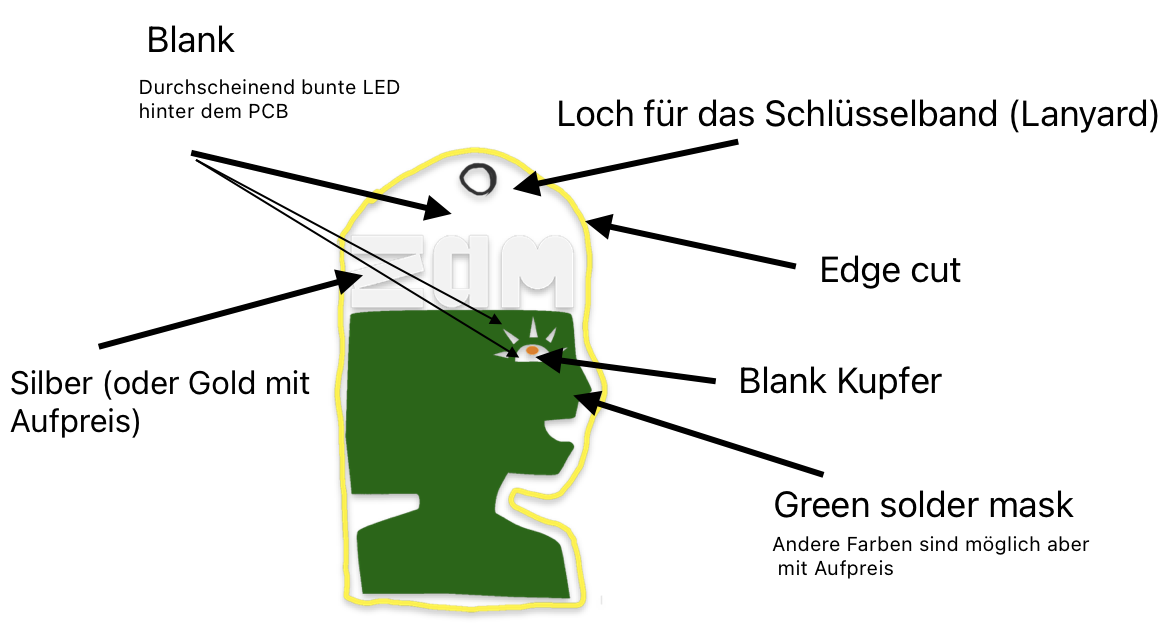
Once I had KiCad available I proceeded to turn the SVG of the graphic into a PCB. To achieve this, the layer feature of Inkscape was invaluable.
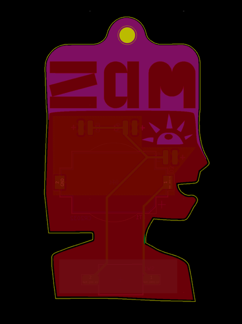
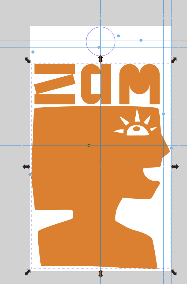 The original image was exported as Front Copper (F.Cu). This will ensure that the section of the board that represents the head and letters will be opaque and not letter any light through.
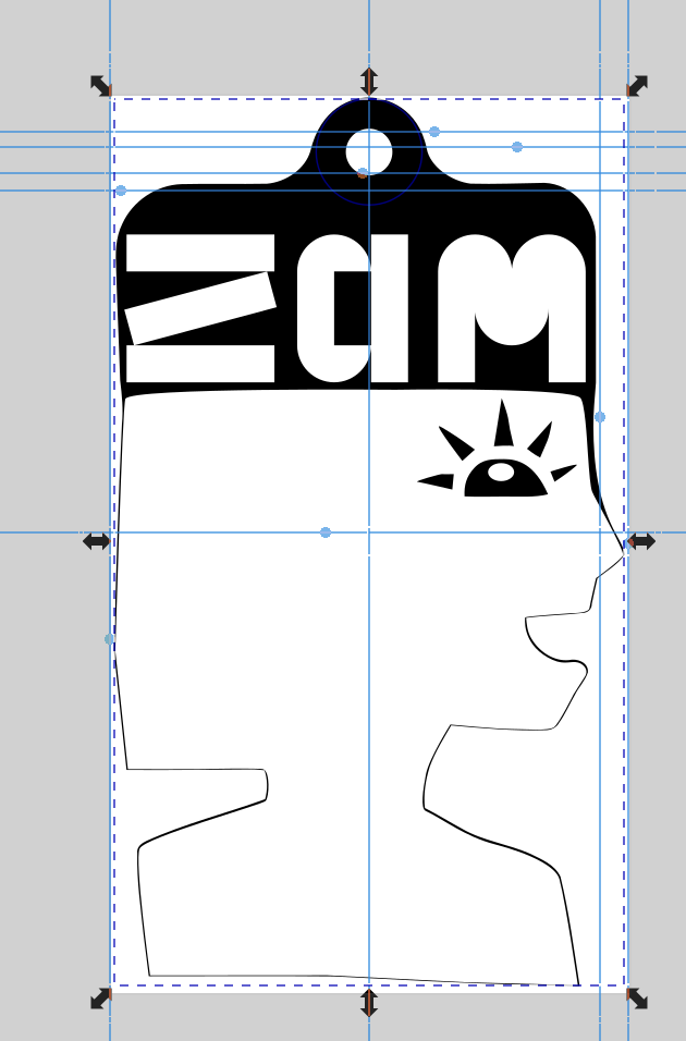 The next layer to export as the solder mask. For the entire image was exported but this has to be converted to a negative since this defines where the solder mask should not go.
 This image is then taken into a graphics program such as GIMP or Krita and trimmed down as the entire outline for this design.
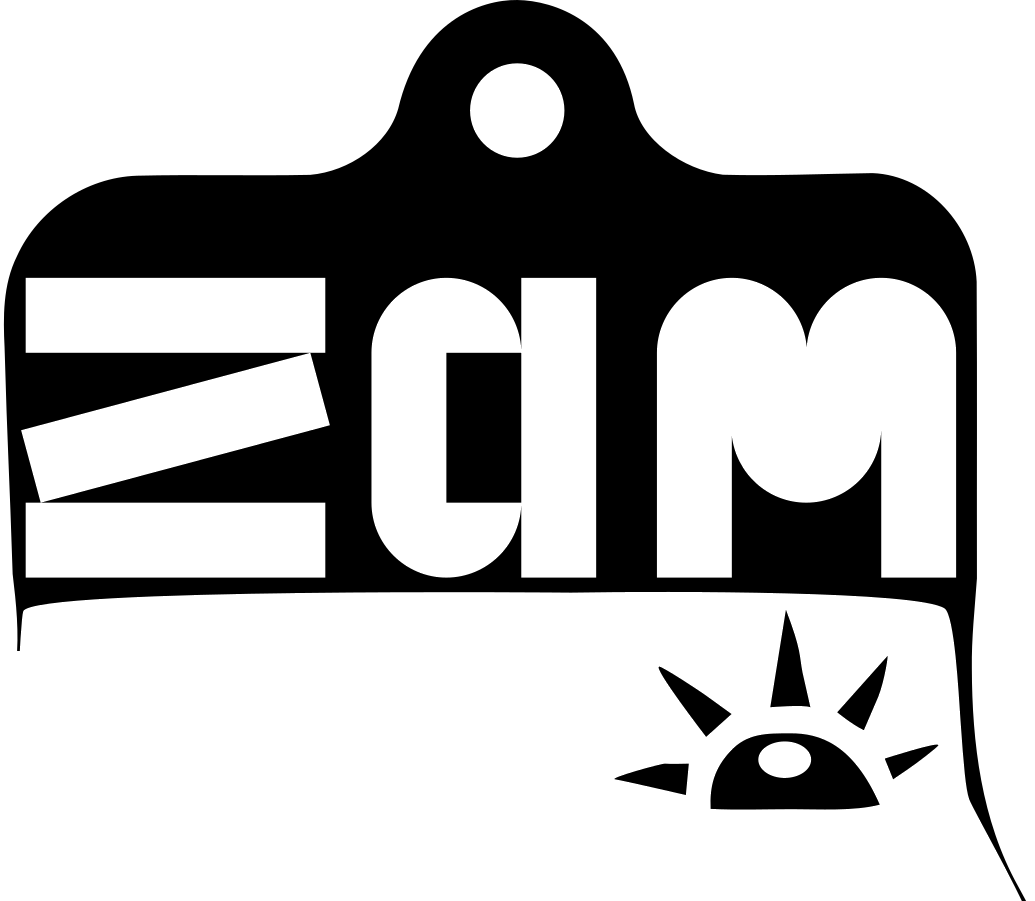
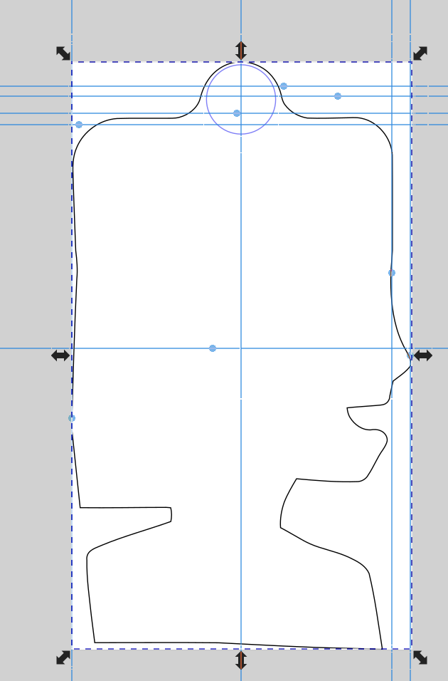 The last layer is based on the entire image and converted to an outline. This is then expanded using the Outset tool. This will ensure that milling tool following the edge cut will not conflict with the actual image outline.
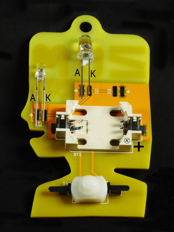
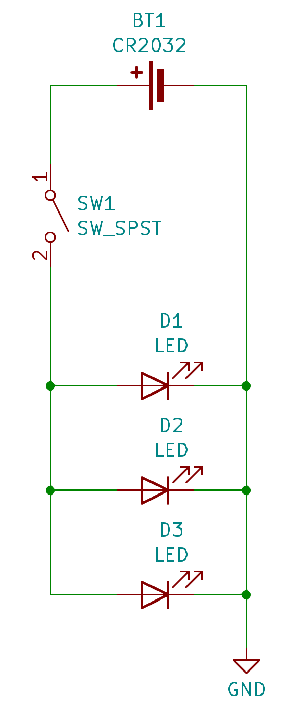
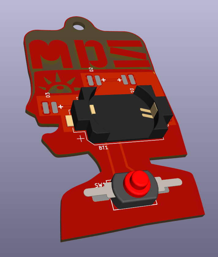
Once the layers are exported and verified, the layout of the board can begin. First of all, a simple circuit is created to defined the required parts. We don't have a lot of time for this project to try things out. So I opted to have space for three LEDs thought I believe only two will be required.
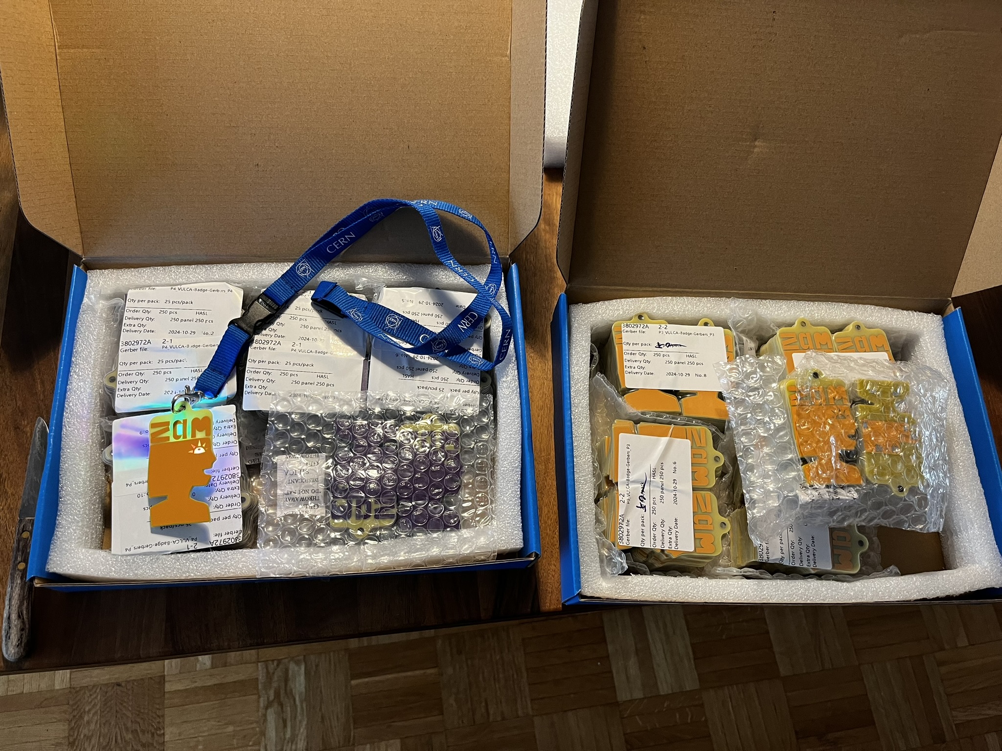
Tag 3. Montage und Prüfung
Bauteile
- 3mm LED
- 5mm LED
- CR2032 Knopfzellhalter
- Schalter