ZAM Badge 2024
Überblick
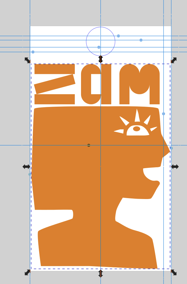
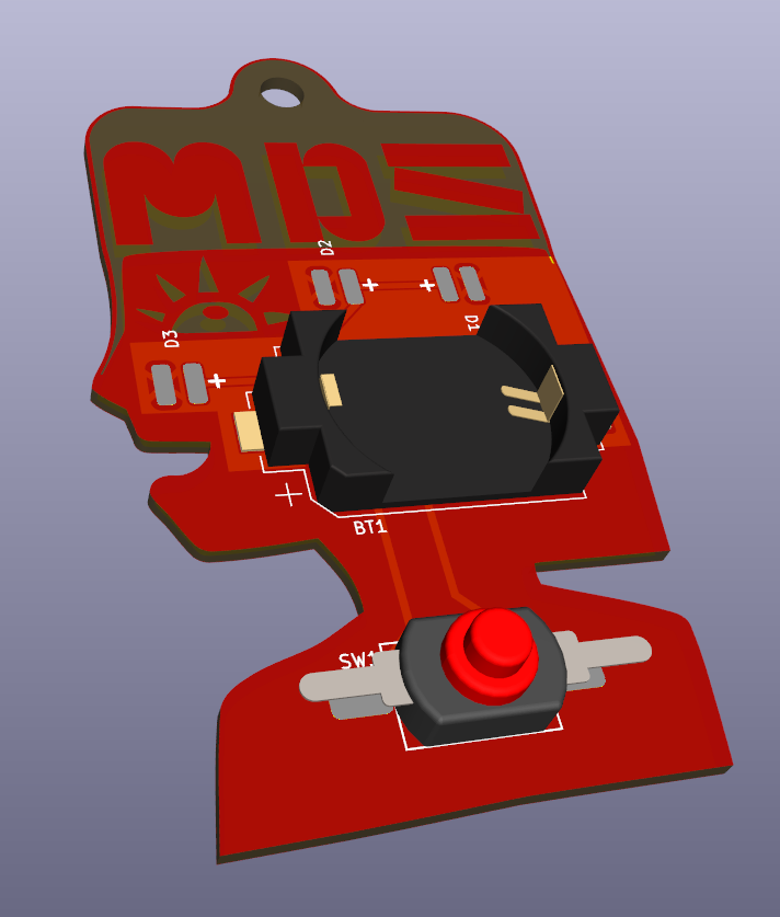
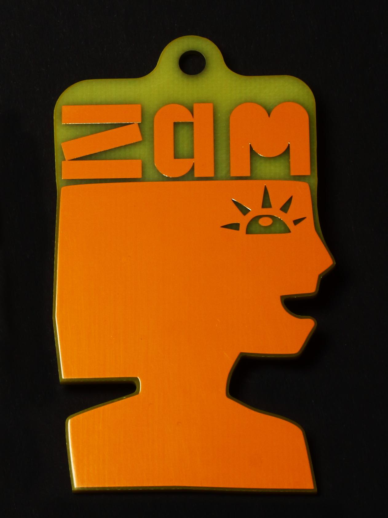
Bei der Planung des VULCA-Treffens kam die Idee eines Badge als Konferenzpräsent und Lötübung auf. Die Idee besteht darin, die folgende Grafik zu nehmen und diese in eine Leiterplatte mit blinkenden LEDs hinter dem Auge und den Buchstaben umzuwandeln.
Projekt-Metadaten
ZAM-Badge-24 GitHub Repository
Jochen Hunger jochen.hunger@betreiberverein.de
Steve Mayze smayze@yahoo.com
Logbuch / Schritte
Tag 1 Zusammenarbeit
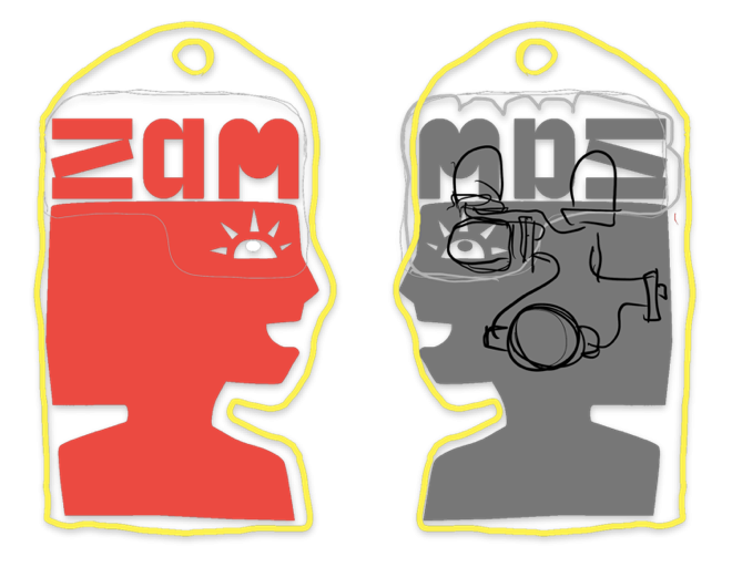
Ich Ihabe haveschon turnedfrüher graphicsGrafiken intoin PCBs before.umgewandelt. IIch waswollte keendieses toProjekt takeunbedingt onin thisAngriff projectnehmen, asda aich feweinige weeksWochen beforezuvor Ian attendedder KiCon Europe 2024 andteilgenommen enjoyedhatte theund talkden Vortrag „WorkingZusammenarbeit withmit artistsKünstlern, toum designschöne beautifulPlatinen boardszu entwerfen.“ Thesehr firstgenossen thinghatte. wasAls toErstes comemusste upich withmir thedas concept.Konzept Givenausdenken. theAuf originalGrundlage graphic,der IOriginalgrafik outlinedskizzierte aich possibleeine arrangementmögliche ofAnordnung theder PCB layers.PCB-Schichten.
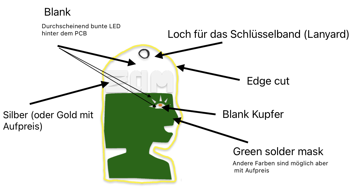
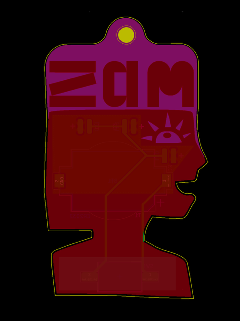
BasedBasierend nauf this,dieser Skizze hat Jochen thendann proposedseine whatVorstellungen hedargelegt. wasDaraus thinking.ließe Thissich wouldrelativ turneinfach outeine toLeiterplatte beentwickeln. fairlyDie straightIdee forwardist, toKopf developund intoBuchstaben a PCB. The idea as too have the head and letters allalle in theder samegleichen colourFarbe zu haben (thedie solderLötmaske) mask)und anddann thenden haveBereich thehinter areaden behindAugen theund eyesum anddie aroundBuchstaben theherum lettersfrei freezu solassen, thatdamit theydie blinkingblinkenden LEDLEDs would shine through.hindurchscheinen.
Idies embellishednoch thisetwas aweiter bitausgeschmückt furtherund withmir myGedanken thoughtsdarüber ongemacht, wherewo thedie componentsKomponenten couldplatziert bewerden placed.
Tag 2. Erstellen des Designs
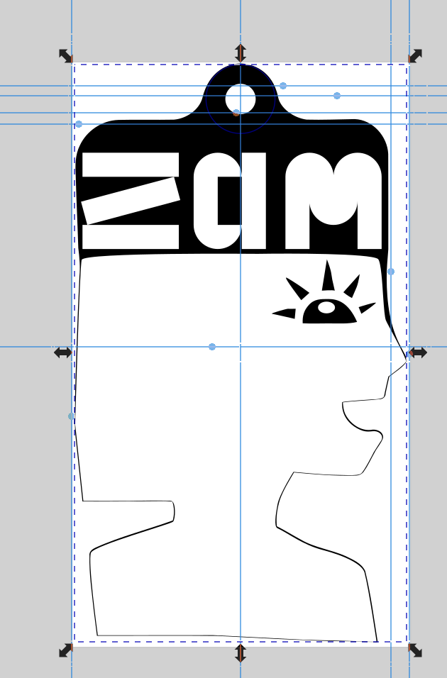
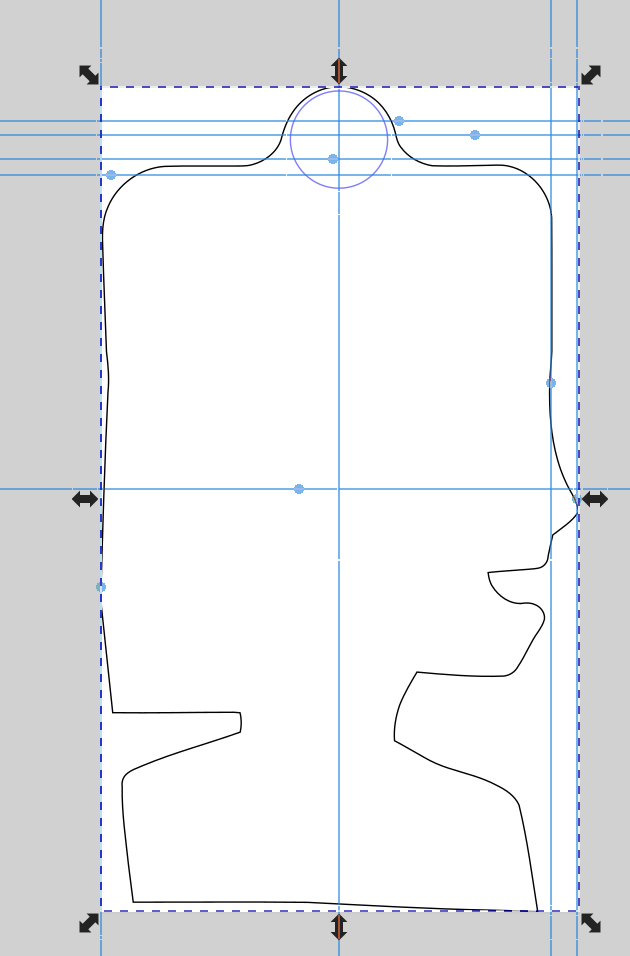
Once I had KiCad available I proceeded to turn the SVG of the graphic into a PCB. To achieve this, the layer feature of Inkscape was invaluable.
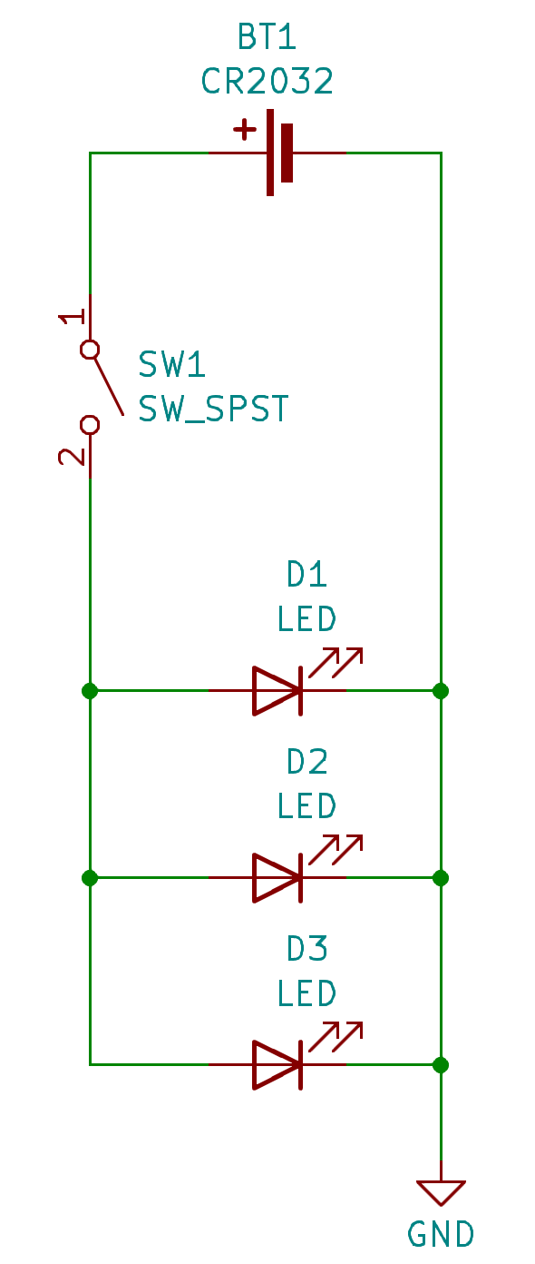
Once the layers are exported and verified, the layout of the board can begin. First of all, a simple circuit is created to defined the required parts. We don't have a lot of time for this project to try things out. So I opted to have space for three LEDs thought I believe only two will be required.
Tag 3. Montage und Prüfung
A week or so after uploading the design files to the fabricator, a panel arrived in the post. I had to assemble to see if there were any issues.
The assembly is quite simple. We start by soldering the LEDs first. The battery holder is large and the LED pads are quite close. There is a risk of damaging the battery holder if the soldering iron should touch it while soldering the LEDs.
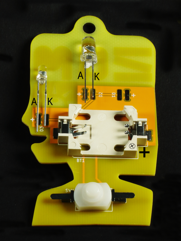
The leads of the LEDs should be bent into place and cut to length. Make sure to take note of the anode and cathode of the LED. These leads need to connect to the appropriate pad. If they are connected the wrong way, you will not damage the LED. It just won't glow. The anode is the longer lead and should be placed on the pad marked with the plus (+) sign.
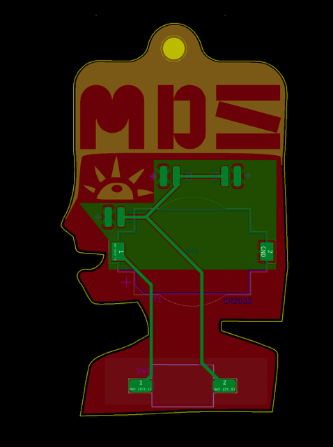
After the LEDs are soldered in place, then the battery holder and switch can be placed on the board. Like the LEDs take note of the orientation of the battery holder. Refer to the graphic below to see the correct orientation. The ⊕ marking on the battery holder should be bottom right as shown in the image.
The switch has no special orientation. The leads will need to be bent into shape so that they neatly touch their pads.
Note that for the battery holder and the switch you might need to apply more heat to get a good connection.
Bauteile
- 3mm LED - eye
- 5mm LED - ZAM letters
- CR2032 Knopfzellhalter
- Schalter

